Solder mask is quite misunderstood when comes to PCBs. It does more than just adding aesthetic value to the PCB. In this article I would like to explain What Solder mask is and why it plays an important role in PCB manufacturing.
What is Solder Mask:
Solder mask aka Solder Resist or Solder stop mask is a polymer that is coated on the the surface of a PCB board. By doing so this polymer will prevent the PCB from degradation due to environmental factors such as moisture, heat etc. With that being said there are three major purposes for Solder mask.
To prevent Oxidation
To prevent solder bridges
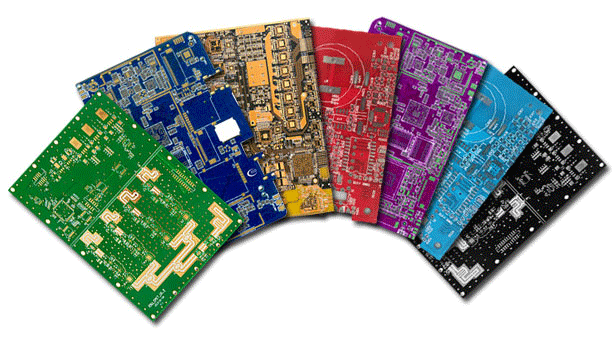
Aesthetic looks
1. To prevent Oxidation:
Oxidation is common problem when comes to metals. With copper traces being metal they are very susceptible to Oxidation. Oxidation on copper traces will affect its current conducting capability and even worse it can lead to short circuit ultimately damaging the board. Thus using Solder mask will seal the copper traces from atmosphere preventing oxidation.
2. To prevent Solder bridges:
Solder bridges refers to the unintended solder flow outside of component that occurs when soldering. These solder bridges will form a connection to nearby traces or pads thus forming a path for short circuit. Solder bridges can highly occur in PCB boards with SMD components which has very little to no space between components and traces. Applying Solder-mask on PCB surface will prevent solder flow out of designated areas thus eliminating the possibility of forming solder bridges.
3. Aesthetics:
Last of all, Solder mask gives aesthetically pleasing look to PCB boards. Green is the most commonly used color but there are other available colors such as Black, Red, Yellow, Blue and so on. Many PCB manufacturers like JLCPCB does not charge extra for different color PCBs.