Multilayer PCB have been around a while now. The rise in demand for compact modern gadgets have really created a huge demand for multilayer PCBs since it saves tons of space. These types of PCBs can accommodate complex designs in a small PCB eliminating the need for big old boards. In case if you are pretty new to multi layer PCBs and wondering what this might be, do not worry! This article will help you to understand Multilayer PCB and point out its most important characteristics.
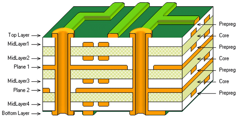
Typical layers in a Multilayer PCBs:
As obvious it may sound, multi layer PCBs consist of more than two conductive layers as shown in the above picture. Conductive layers are the ones which actually carry the current in and out of all components within the circuit.
In a multilayer PCB excluding the top and bottom layers others are named as Mid layer 1, Mid layer 2 and so on. Similarly we also have Internal plane 1, Internal plane 2 and so on. These naming conventions will allow users and PCB manufacturers to design and manufacture their boards precisely.
Apart from the conductive layers Core and Prepreg forms multi layer PCB board.
Core:
This is the layer on which the conductive layer or copper traces sits on. Most common core material is FR-4. This is made up of fiberglass, usually will be in the form of a sheet. Core gives the PCB its form and shape.
Technically this is similar to core material but not cured through heat like core material. So rather than being a rigid sheet it resembles a thin film that will be placed in between the core and conductive layer. The function of Prepreg is to act like a glue that bonds the copper traces in the conductive layer to the core.
Midlayer:
This is the conductive layer that is placed between the top and bottom layer in a multi layer PCBs.
Internal plane:
This also a conductive layer that is placed between the top and bottom layers. But the key difference is that this layer has signal planes such as VCC, GND and other signals based on designer needs.
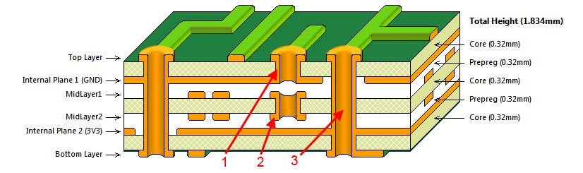
Connectivity:
The connectivity between layers established by three different types of vias.
Blind Via: These types of vias (1) connect Midlayer or Internal plane layer to Bottom or top layer in a multilayer PCBs
Buried Via: These types of vias (2) are buried within the layers and connects Midlayers to Internal plane in a PCB. This via will not connect to bottom or top layers.
Through hole Via: This type of via (3) connects top and bottom layer and layers within them.
I would take this time to give a shout out to JLCPCB for their impeccable PCB manufacturing and assembly services. P.S : They are capable of manufacturing 1 – 6 layer PCB boards.
Hope this tutorial shed some light about Multilayer PCB. Do you have something to share about Multilayer PCBs, share your thoughts in the comments section below.