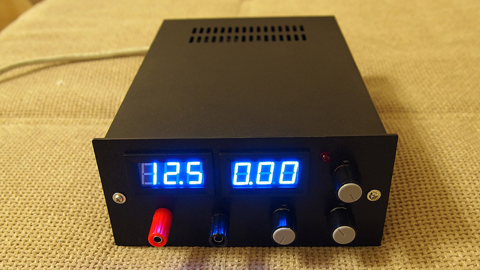
Every lab needs to be equipped with essential equipment. Out of all I would say power supply is most important since it powers up the projects. Batteries, DC adapters can do fine job but as demand grows and project gets bigger a professional and adjustable power supply becomes a necessity. To cater that I have designed an adjustable 50V / 5A power supply with a variable output from 0V to 50V and adjustable current limiting from 0A to 5A. Most simple power supplies cant get the output to come down to exactly 0V or 0A. But in this circuit, the differential amplifiers have a negative power supply rail at (-3V), which can pull the output down to exactly zero.
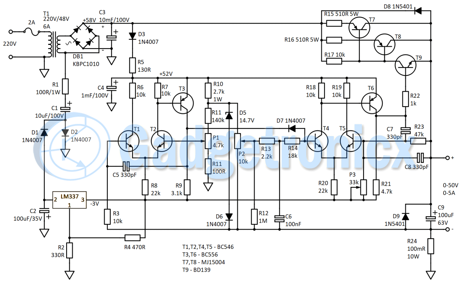
CIRCUIT DIAGRAM OF BENCH POWER SUPPLY:
WORKING:
The power supply relies upon two differential amplifiers made out of Transistors T1 to T6. The first one being responsible for controlling the output current limiting. The second differential amplifier controls the output voltage. They both are driven by the reference voltage created by D5 and D6. The use of zener and a normal diode is to compensate for thermal drift of reference voltage generator. This is because they both have opposing thermal coefficients.
VOLTAGE CONTROL CIRCUITRY:
The voltage control circuitry is created from Transistors T4,T5 and T6. This works by measuring the differential voltage on base terminals of T4 and T5. One terminal is supplied with reference voltage, and the other terminal with some of the output voltage. The reference voltage created by diodes D5 and D6 is around 15.4V. Hence the differential amplifier must amplify the voltage difference by 3.4 times to match the 50V output. This is done by the voltage divider (R23,P3) connected to the inverting terminal of this differential amplifier, setting the gain to 3.4 times of input signal.
When tweaking the power supply, you must set potentiometer P2 to its upper most level. Then fine tune the maximum output voltage to 50V by P3. Since the current sensing resistor (R24) is in a low side configuration, the differential amplifier must correct for the voltage drop it makes when power supply is loaded. This is why the reference voltage generator is connected to the (-) terminal of the power supply and not ground terminal. By connecting the reference voltage generator in such a way, it allows it to drift up or down by the same amount of voltage the current sensing resistor creates as a voltage drop. Therefore it keeps the output steady through the load.
CURRENT LIMITING CIRCUITRY:
The current limiting circuitry is comprised of Transistors T1,T2 and T3. This works by measuring the voltage drop created by current sensing resistor and comparing it to a given reference voltage created by R11 and P1. I actually suggest replacing R11 with a 220k trimmer and fine tuning the maximum current limit to match your requirements.
As it is, the protection is set to enable at 5.3A. With an adjustable value for R11, you can set the protection at any level up to maybe 6-7A without compensating the circuit for increase in power. When the protection is ON, T3 drops the voltage at its collector, thus creating an appropriate potential difference through the diode D7. At this point it starts stealing some of the biasing voltage of T4. By dropping the base voltage of T4, output voltage drops sufficiently to keep the current through the load constant.
GERBER FILES:
A big thanks to Morne Stander for designing PCB for this circuit and sharing it with the community. You can download the Gerber files below



VOLTAGE DOES NOT HOLD STEADY,