PCBA – Printed Circuit Board Assembly is relatively a new term where manufacturers provide the service of assembling the components in the PCBs in addition to manufacturing them. PCBA includes steps like solder paste printing, mounting small and large components, reflow soldering, wave soldering, etc. This article explains the process of PCBA in detail.
SMT and THT in PCBA Manufacturing:
PCBA means “PCB assembly” or “assembled PCB”. When a printed circuit board is mounted with required electronic components, we call it a PCBA. A complete PCBA manufacturing process needs two assembly procedures – an SMT (surface mount technology) assembly and a THT (through-hole technology) assembly.
These days most of the designs use SMT components such as Inductors, resistors, compactors, ICs, etc. They can be soldered on pads of the board using solder paste. A reflow soldering oven melts the solder paste and connects the SMT components with the board tightly.
The components which has the legs (THT components ) to insert in to the board’s drill holes and need to be assembled after the SMT assembly. Technicians use hands or machines to insert the component legs and then the assemblies go through a wave soldering oven to connect the THT components with the board. This process is called THT assembly.
When printed circuit boards are ready, you need to have them assembled with components. Usually, a PCB company doesn’t produce components but sources from their trusted suppliers. You can buy all components on your own and send them to the PCB company to assemble, or provide special components and source basic components from the PCB company.
At PCBONLINE, all basic components are stored in their warehouse and ready to use at once, and they also source special custom-made components. When circuit boards and components are available, let’s start to manufacture PCBAs.
Complete Process of PCB Manufacturing in PCBONLINE:
Step 1. Preparation – Checking Bill of Materials
Bill of Materials (BOM) is an excel containing all your components information. When you order from a PCB assembly company, you need to provide the BOM. Not all assembly companies check your BOM and this may lead to failures. But PCBONLINE does, and it is free. An experienced engineer checks your board design, the component samples, and your BOM carefully. If everything is okay, the assembly starts.
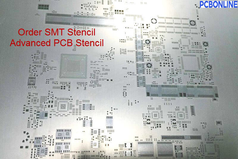
Step 2. Manufacturing PCB Stencils for PCB Assembly
PCB stencils are also known as SMT stencils, they are used for the surface mounting. When engineers check your BOM, PCB stencils are also made. Standard solder paste thickness ranges from 0.09mm to 0.15mm, and the SMT stencil thickness has to be within the tolerance of ±0.03mm thicker than the solder paste thickness. How many stencils are manufactured depends on how many SMT lines are open to assemble your boards in a PCB assembly factory.
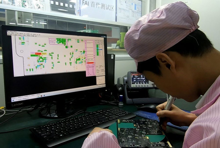
Step 3. Manufacturing a PCBA Sample for First Article Test
First article test (FAT) is necessary for mass PCBA production because if minor mistakes happen, the whole large batch of PCBA become failures. So PCBONLINE assembles the first piece of board to test its specifications and generate an FAT report for customers to review. If the PCBA is good and customers approve, then the PCBA manufacturer starts batch production. The PCBA sample and FAT are free of charge for customers.
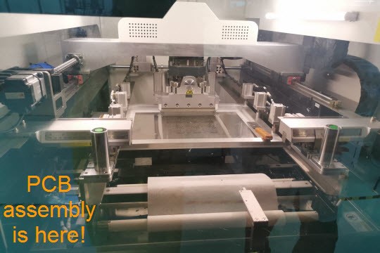
Step 4. Begin PCBA Batch Production – Solder Paste Printing
Functional testing to electronic components is conducted right before the assembly where printed circuit boards are sent the auto loader. When technicians make sure that the assembly line is ready, all machines are powered on. The boards are then sent from the auto loader to the solder paste printer. A blade carrying the solder paste presses the PCB stencil, and the solder paste filters the stencil holes and prints on pads of the PCB. when the board is pasted, it leaves the printer and the next board is printed.
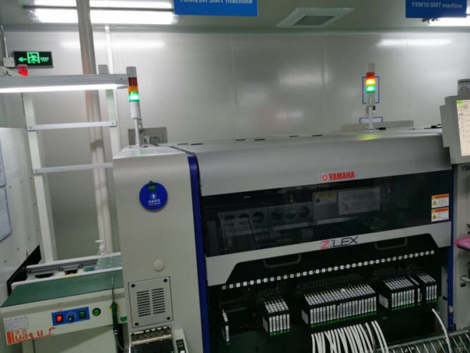
Step 5. Mounting Small Components
Small components are the SMD components which will be small in size. Some of the small component package sizes are 0201, 0402, 0603, etc. When the board is sent into the high-speed mounter, these components are quickly picked and placed on their desired PCB pads. Then the board mounted with small components leaves to the functional mounter and the next board comes in.
Step 6. Mounting Large Components
Large components are the SMD components large in size, like BGAs, FPGAs, ICs, USB, connectors, etc. Like in the high-speed mounter for small components , larger components goes to the functional-mounter, where the components are picked and placed on the required pads. Here the machine operation will be much slower and more accurate. When the board leaves the functional mounter, it has to pass the solder paste inspection (SPI) to make sure the solder paste thickness and shape on pads are qualified.
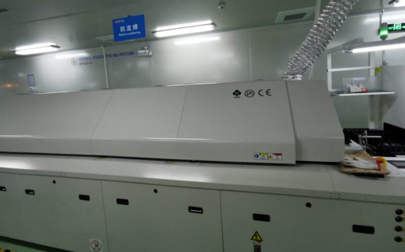
Step 7. Reflow Soldering
In this step, the boards pass the reflow oven and the solder paste melts and solidifies. In this way, the SMD components and the board are connected both electrically and mechanically. When the boards leave the oven, they have to go through an automatic optical inspector to check whether the mounting is qualified. If the assemblies are qualified, they head to the next line.
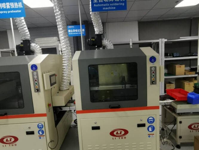
Step 8. Through-Hole (THT) Assembly
The above is for SMT assembly, and here is the THT assembly line. SMD components can be “printed” on the circuit board, but components with long legs can’t and they have to insert the through-holes. This operation can be completed either by machines or by hand as it is quite simple.
Step 9. Wave Soldering
THT assembly only inserts the component legs through holes loosely and the purpose of this step is to connect the THT components tightly to the PCB. The assemblies go through a pre-heater to warm up, and then go through the wave soldering oven. In the oven, the liquid tin fill the gaps between the THT component legs and the board. When the PCB leaves the oven, the tin solidifies and then the THT components are connected tightly to the assembly electrically and mechanically. Then technicians trim the THT legs to 1mm to 2mm’s long.
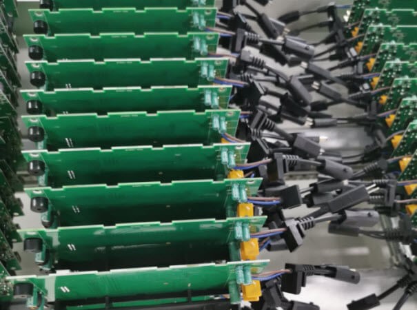
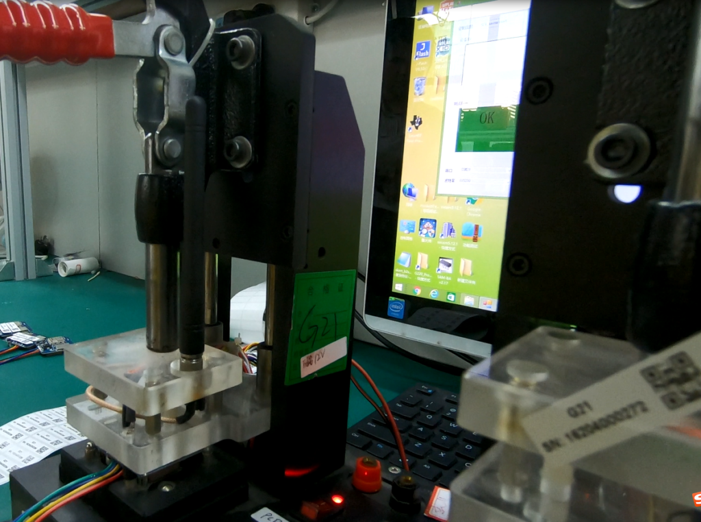
Step 10. PCBA Functional Testing
During PCBA manufacturing, PCBA testing’s are necessary in case of soldering defects to avoid economic losses due to re-assembly. At PCBONLINE, the functional testing is free for customers. Technicians use a functional tester to test the current, voltage, and so on while the PCBA is powered on. If the PCBA works well, then technicians conduct the thermal aging test. Then it is assembled with the outer shell and packaged for delivery.
Why PCBONLINE is a Reliable PCBA Manufacturer
If you’re looking for batch PCBA manufacturing, you need to work with a reliable PCB assembler. PCBONLINE is highly recommended for the high-quality assembly, complete PCBA testing, and fast delivery. You can register for free and get a quote online, or contact info@pcbonline.com for a quotation.