
Transistor is a popular three terminal semiconductor device used in Switching and Amplification applications. Modern electronics we use today made possible because of transistors since it played a huge role in reducing the size of boards drastically. This tutorial covers
- Construction of BJT transistor
- Working of transistor
- Operating regions of transistor
- Applications of transistor
Must read: Resources to self learn Electronics
Construction of BJT transistor:
![]()
Bipolar Junction Transistor is a three terminal semiconductor device constructed by joining three semiconductor materials together. This construction of N-type , P-type, N-type semiconductor materials creates two possible transistor configurations. First one is NPN transistor where the device is put together in N-type, P-type and N-type configuration whereas in PNP transistor the device is combined in the following fashion: P-type, N-type and P-type materials as shown in the figure above. This is quite similar to the construction of a diode where two semiconductor materials such as P type and N-type joined together whereas in transistor these materials are either two P-type with one N-type in the middle or two N-type with one P-type in the middle.
The terminals attached to NPN or PNP transistors are Collector, Base, Emitter. These terminals need to be used by the user to operate the transistor. The important thing to note in the above diagram is that Area of Emitter, Base and Collector are not equal in size. Base region will be smaller comparing to Emitter and Collector. Area of Emitter is bigger than Base but smaller than Collector. Collector forms the largest region in a BJT. Size of the regions in a BJT follows this: Base < Emitter < Collector. The reason for this design is to facilitate current flow between Emitter and Collector, this will be explained below.
Working of BJT transistor:
![]()
As stated earlier, BJT transistor is a device that is made by joining N-type, P-type and N-type doped semiconductor materials together. In case of NPN transistor. N-type semiconductor has electrons as majority carriers and for P-type semiconductor it will be holes. We will use NPN transistor as reference to explain its working throughout this article. The second most important characteristic of a transistor other than the width of semiconductor region is concentration of doping levels, the three regions are not linearly doped. The Emitter N-type semiconductor is heavily doped hence has most number of charge carriers as shown in the above diagram. Base P-type is moderately doped and Collector N-type has lowest doping levels. The concentration of doping level in NPN transistor will be: Emitter >Base >Collector. This leaves more number of free electrons to move from Emitter to Base and to Collector of the BJT transistor.
Working of transistor is very much similar to diode since there is a significant resemblance in construction of diode to transistor. Diode has two (N-type and P-type semiconductor ) material combined together. However in a BJT transistor there is three regions involved but working principle remains same.
Depletion Region:
![]()
The process of making a BJT transistor that is combining N-type, P-type and N-type material together will form two transistor junctions – Emitter and Base ( BE ) & Base and Collector ( BC ). Working of transistor can be understood by understanding how charge carries behave within its three regions. When combined the electrons from Emitter ( N-type material ) will diffuse into Base ( P-type material ) since concentration of charge carries in Emitter is higher than Base. In base electrons from Emitter will combine with holes in Base to form electron hole pairs. When electrons move from emitter this leaves an empty place, this will be occupied by movement of holes from Base region. This process of diffusion occurs until diffused electrons and holes oppose further movement of charge carriers to other sides as shown in the above figure.
The diffusion process leaves the area close to the junction with no electrons or holes (charge carriers ) forming a region which is referred as depletion region. Since this depletion region lacks charge carriers, it serves as a barrier to movement of charges between regions. This leads to development of a voltage potential of 0.7v across the depletion region. This means a voltage more than 0.7v should be applied to get the charge carriers move through BE depletion region.
There is another depletion region that is formed in the junction BC due to the process of diffusion. The depletion region in BC junction is larger than depletion region of BE junction. This is because of the different doping levels in the Emitter, Base and Collector region of a BJT transistor. We already knew when N-type and P-type regions are combined diffusion occurs, this leads to exchange of charge carriers between two regions. Since the doping level of Emitter is higher than Base even after diffusion more number of electrons will remain in Emitter which leads to a small depletion region in which charge carriers will be non existent. Similarly Base will have a depletion region which is bigger than Emitter.
However Collector being the region with least doping level after losing electrons due to diffusion, the depletion region formed will be large compared to Base and Emitter. Therefore the depletion region formed between the junction Base and Collector BC, will be significantly larger than the depletion region formed between the junction of Base and Emitter BE.
Base current and Emitter current:
![]()
To understand the working of transistor let’s consider the most important characteristics of a BJT transistor. When a small current is supplied to the base of a transistor, it allows higher current to flow from Emitter to Collector considering the actual direction of current flow. This is the principle behind using transistor as a switch. Consider the above diagram where a supply voltage is connected between Base and Emitter and another source is connected between collector and emitter. Voltage supplied here at BE should be more than 0.7v to initiate current flow since voltage potential developed across depletion region BE is 0.7v. When this happens electrons from emitter will start crossing depletion region and enters base and recombines with holes in the base.
Note: In the above diagram recombination of electron hole pairs was omitted for the sake of simplicity since electron movement is the subject of interest.
![]()
Now the the electrons from power source connected across VCE and Emitter will be too high and there won’t be enough holes in base to recombine. At this point some electrons flow through the base to the positive terminal of the voltage source VBE. This is the base current. The leftover electrons which is high in number will get attracted by the positive terminal of the voltage supply VCE. This forces the electrons to move past BC depletion region. This will initiate a flow of current from emitter to collector which is the collector current. This collector current will be comparatively larger than the base current since more number of electrons will move from Emitter to Collector than the electron movement from Emitter to base. The above steps collectively make the transistor to operate like a switch.
As explained above, the collector region receives the majority of electrons from emitter and the base. Therefore Collector region needs to dissipate more heat than other regions. This is the reason for designing BJT collectors with large surface region.
Operation regions of BJT transistor:
The next important thing to be familiar with BJT transistors are their Operating regions.
The transistor can be operated in four regions. The operating region decides the application of the transistor. The four operating regions of a BJT transistors are
- Cutoff region
- Saturation region
- Active region
- Breakdown region
The operation regions mentioned above relies on three important parameters of a transistors. These are Collector Emitter voltage VCE, Collector current IC and Base current IB. Controlling these three parameters will allow us to use transistor in the desired region.
Cut off region:
Image courtesy: www.electronics-tutorials.ws
This is the region where transistor will be in Off or Cut off state. Transistor will allow current to flow from Emitter to Collector ( actual current flow ) only when base to emitter voltage VBE exceeds 0.7v, which enables Base current to flow. Therefore transistor is said to operate in Cut off region when voltage VBE applied at Base and Emitter is less than 0.7V and no current flows through base.
The above graph will help you to understand this better. The shaded region highlighted in pink in the above graph represents Cut off region. It shows that there is zero base current and VBE is less than 0.7V. The transistor will remain in cutoff region even when Collector to Emitter voltage VCE is increased. Therefore when the base current is zero any increase in Collector to Emitter voltage VCE does not impact the Collector current in any way and transistor will be in off state as long as base current is zero.
Conditions to operate transistor in Cut off region
IB = 0
VBE < 0.7v
Saturation region:
This region of transistor can be best described as contrary to the cut off region. In cut off region there will be zero current flowing through Collector and Emitter. However in saturation region maximum current will flow without any regulation through Collector and Emitter junction. This maximum current depends on the power supply and load’s capability. It is the designer responsibility to ensure that collector current IC does not exceed the maximum current rating of the transistor in use. Each transistors will be rated to withstand certain collector current and it differs from transistor models and manufacturers.
If you look at the below graph the blue shaded section represents the saturation region.
Image courtesy: www.electronics-tutorials.ws
To operate transistor in Saturation region base terminal should be forward biased which means VBE > 0.7v. This will force Base current IB to flow from Emitter to Base. This current will influence the next key parameter, that is Collector Emitter voltage VCE and force the transistor to operate in saturation region.
When the base current was zero, VCE will be equal to applied voltage VCC. As soon as Base current starts flowing VCE will be equal to or less than VCEsat which is the collector emitter saturation voltage. This VCEsat may range from 0.1V to 0.7V depending on the transistor manufacturer and model. The reason why VCE goes below VCEsat is that when no current flows through base, current flow from emitter to collector will be zero. Therefore voltage at the collector will be maximum or equal to the VCC. However when current flows through base it initiates current flow from Emitter to Collector. At this point there will be virtual short circuit since current flows from emitter to collector.
Conditions to operate BJT transistor in saturation region:
IB > 0
VCE < VCEsat
VBE > 0.7v
Active region:
This is region that exists between Cutoff and Saturation region. In saturation region collector current flow will be maximum however in active region, collector current IC can be controlled by base current IB. Here the collector current that is flowing from emitter to collector terminal will be controlled by the base current IB. Therefore this region will be useful when user wants to use BJT transistor as an amplifier.
Image courtesy: www.electronics-tutorials.ws
The relationship between base current IB and collector current IC is decided by Gain ( β ) of a transistor. It is also referred as hfe in many instances. The β value of a BJT transistor can range anywhere from 10 to 2000 depending on the transistor manufacturer and model. A β value of 100 is common and prevalent among transistors. The relationship between base current, collector current and β is given by the formula
IC = β x IB
Looking at the below graph you can see how collector current IC varies with different input base current. This is called as characteristic curve of a transistor. In the given graph 2uA of IB will force the Collector current to raise to 20mA and similarly 3uA of base current forces the collector current to 30mA. Using the above formula we can deduce that the β value of the given transistor is 100
β = 30mA / 3uA = 100
From this we can deduce in active region of a transistor, collector current will vary based on base current and gain of a transistor. Adding to this, another important characteristic of active region is that increase in collector voltage will have no influence over the collector current. As you can observe from the graph, the collector current does not change for a given base current and remain steady despite raise in collector voltage.
Another important factor for BJT transistor to operate in active region is that Base voltage VB should be greater than Emitter voltage VE ( VB > VE) but should be less than collector voltage VC ( VB < VC ). Also the collector voltage should be greater than Collector to Emitter saturation voltage. VCEsat.
Conditions to operate BJT transistor in Saturation region:
VC > VB > VE
VC > VCEsat
Breakdown region:
In this region the transistor ceases to work or it will breakdown. Remember we have discussed in saturation region section, that collector current in a transistor will be dependent on factors such a collector voltage and load used ? A transistor will enter the breakdown region when this applied collector voltage exceeds maximum rating of a transistor. Consider a transistor which is rated to operate at 30V as its maximum permissible collector voltage. Here applying voltage beyond 30V to its collector will allow large undesired current to flow through the collector terminal and ultimately destroys the transistor. Circuit designers should design their circuits in a way that transistor never enters the breakdown region in their design.
Common applications of BJT Transistor:
Transistor is most commonly used in two applications
- Transistor used as a switch – Transistor operates in Saturation region and Cutoff region.
- Transistor used as an amplifier – Transistor operates in Active region.
BJT Transistor as a switch:
Transistor is popularly used as a switch where a high current load need to be turned ON or OFF by a small signal current. When using as a switch transistor will either operate in Cutoff ( OFF ) or Saturation region ( ON ). Imagine you are using a microcontroller and you need to drive a DC motor which draws 200mA of current for its operation. For a microcontroller its impossible to source such huge current to drive the motor directly. This is where transistor will be used to switch the large load, DC motor in our case using a small source current from the Microcontroller.
![]()
The above circuit diagram shows how to use transistor as switch in your circuit. Here the transistor operates in the saturation region, which means large collector current flows through the base of transistor to emitter and then to ground upon small signal input current flow into the base. Read the section – Saturation region of transistor to get more clarity on this.
To turn ON the transistor or operate it in saturation region, the base emitter voltage need to be greater than 0.7V (junction voltage that is necessary to move charge carriers across depletion region ). High logic from Microcontroller will be typically +5v or +3.3v and this is sufficient to drive the Base Emitter BE junction. When output voltage from Microcontroller goes low or 0v bias voltage will be removed and thus transistor will be turned OFF or pushed into cutoff region.
Another thing to consider is the amount of base current. Even though the collector current is not influenced by base current some conditions need to be satisfied in order to saturate and cutoff the transistor successfully. In saturation the base current IB < β x IC, also the ratio between IC / IB should be optimum enough to quickly switch between Saturation and Cutoff region. As a rule of thumb base current is chosen to keep the ratio IC / IB as 10 for faster turn ON/ OFF of the transistor. Also the base current should not exceed more than maximum rated base current of the transistor. Therefore a resistor is used to limit the base current as well to provide bias voltage to force the transistor to operate in saturation region.
Let’s say the DC motor consumes 100mA current. This means our base current has to be about 10mA. We will use the ohm’s law to fix the base resistor.
R = ( VIN – VBE ) / IB
= ( 5 – 0.7V ) / 10mA
= 430 ohms
BJT Transistor as Amplifier:
Amplifiers are devices that is used to amplify or increase the amplitude of important parameters of a signal such as Voltage, Current or Power. Transistors popularity skyrocketed since it can operate as amplifier despite its size and cost. To operate Transistor as an amplifier it has to configured using passive components such as Resistor, Capacitor and Inductor. While there are many possible ways of building a transistor amplifier it can be broadly categorized into three common configurations.
Common Emitter configuration of Transistor (CE):
Common Emitter configuration of a transistor refers to the transistor configuration in which emitter terminal will be common to both input and output signal. Here input is applied between Base and Emitter, Output is drawn from Collector as shown in the below diagram. Also AC signal goes to ground through Emitter. Hence this configuration is known as as Common Emitter configuration.
Steps to design a Common Emitter Transistor amplifier:
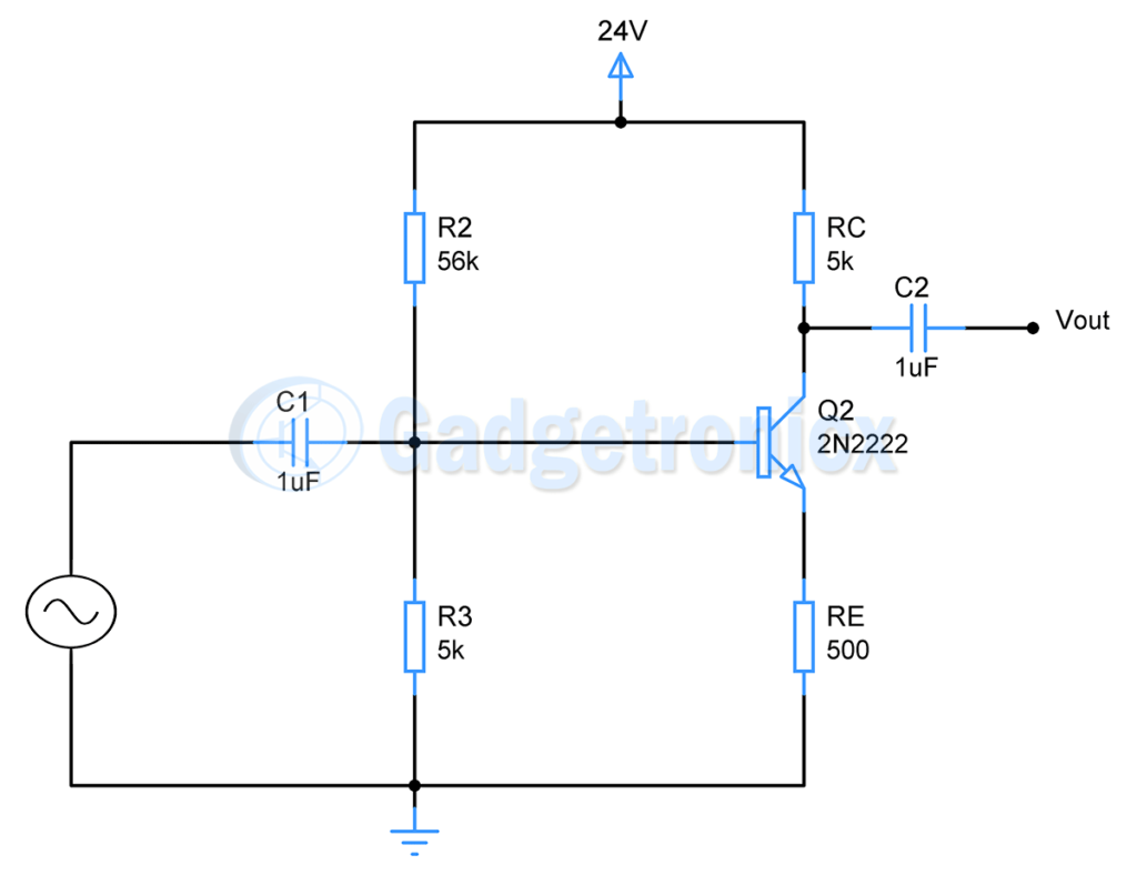
To operate transistor as Amplifier, bias voltage needs to be applied at the base. Here resistors R2 and R3 forms a voltage divider and sets biasing voltage to Transistor. C1 is a coupling capacitor which filters out any undesired DC element in the input signal. C1 will also prevent DC bias voltage from reaching the AC voltage source.
- As a start we will fix the output impedance and output current of our CE amplifier. The best practice is to match the impedance of the load that we are going to use with the amplifier. As an example we will fix the load impedance RC as 5000 Ohms.
- The best practice is to fix the collector voltage as half as supply voltage since this will allow input signal to achieve maximum and equal swing with 0V being negative peak, 12V being DC line and 24V being positive peak. Hence we fix the collector voltage as 12V.
- The collector current IC can be calculated using the formula
IC = ( 24V – 12V ) / 5000 = 12V / 5000 = 2.4mA
4. The Emitter resistor RE should be chosen in a way that is 10 times less than collector resistor RC.
RE = RC / 10 = 500 Ohms
5. The current through the Emitter of an amplifier will be close to the Collector current ( IC = IE ), hence we will use the collector current to obtain Emitter voltage using Ohms law
VE = IE x RE = 2.4mA x 500 = 1.2V
6. The Base bias voltage of the transistor has to be 0.7V greater than Emitter voltage. This is because of the forward voltage drop from Base to Emitter terminals, the base voltage VB will be
VB = VE + 0.7V = 1.9V
7. As stated earlier the resistors R1 and R2 is used to build a resistor divider to provide sufficient bias which is 1.9V to the base terminal. To do that we will determine the resistor R2 value first. Ideally R2 should be less than Zin which is the input impedance given by B x RE / 10. Therefore R2 should be less than
R2 = Zin / 10 = β x RE / 10 = 5000 Ohms
8. The base current when the gain is 100 can be given using the gain formula
IB = IC / β = 2.4mA / 100 = 0.024mA
9. To calculate the current through R2 we can use the following formula
I2 = VB / R2 = 1.9V / 5000 = 0.38mA
10. Using the IB and I2 we can calculate the current flow through R1 which forms the voltage divider along with Resistor R2.
I1 = I2 + IB = 0.024mA + 0.38mA = 0.41mA
11. Now that all it is left is to calculate the value of R1. With the values of Vcc, I1 and using the below formula we can calculate R1
R1 = ( VCC – VB ) / I1 = ( 24V – 1.9V ) / 0.41mA = 53.9K
We choose a 56K as a standard value resistor for R1.
In this configuration output signal possess high current than input signal. The voltage gain of the output signal comparing to input signal will be significantly higher as well. This makes CE configuration a great choice for obtaining high power gain in the output. Another key thing to note with this configuration is that the input signal will undergo 180° phase shift in the output. This means the polarity of the input signal will be reversed in the output signal.
Common Base configuration of Transistor (CB):
Common base configuration of a transistor means that base of a transistor will be common to both the Input and output signal. Here the base terminal will be usually connected to ground or fixed voltage reference will be used by both input and output signal.
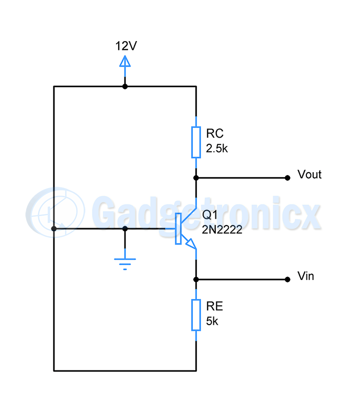
The input signal is fed between transistors base and emitter terminal as shown in the above diagram. The input resistance in CB amplifier will be low. Here input current IE will be higher than the current of output signal IC owing to high output resistance. Therefore emitter current can be given as
IE = IB + IC
The ratio between Collector current and Emitter current can be given as
Alpha = IC / IE
Since we have already established collector current will be less than Emitter current, Alpha will be always less than one. In fact it will be close to 1 in the range of 0.9 .
On the other hand voltage of the output signal will be higher than the voltage of the input signal. The voltage developed across collector resistance RC is the output voltage in CB amplifier. Using Ohms law we will be able to deduce the output voltage
VC = IC x RC
The gain of CB amplifier can be deduced using the gain formula
AV = VOUT / VIN = VC / VE = ( IC x RC ) / ( IE x RE )
Since IC / IE is Alpha we can rewrite the above formula as
AV = Alpha x RC/ RE
Another factor to consider in the design of CB amplifier is the dynamic emitter resistance. This is the resistance exhibited by the emitter diode junction. This is given by r’e = 25mV / IE. 25mV is the thermal voltage of the PN-junction and IE is the Emitter current.
The influence of dynamic resistance to the gain will be higher than emitter resistance RE, since RE will be much higher than r’e. Therefore the voltage gain can be rewritten as
AV = RC / r’e
Consider a signal of 500mV / 1mA is fed into the emitter terminal. Then r’e will be
r’e = 25mV / 1mA = 25Ohm
Now calculating the voltage gain using the r’e value
AV = RC / 25
Let’s fix our desired gain as 100 to calculate the RC
100 = RC / 25
RC = 2.5K
The voltage output across collector terminal will therefore will be
VOUT = VIN x AV = 50mV x 100 = 5V
Given the VCC is 12V the voltage amplification of the signal is optimum and provides full swing to the signal.
Common Collector configuration of Transistor (CC ):
Common Collector configuration is used when high current gain in the output is necessary. This amplifier resembles very much like a common Emitter amplifier except the terminal from which output signal is derived. In common emitter configuration output signal is derived from collector terminal across resistor RC whereas in common collector configuration output signal is derived from emitter terminal across resistor RE. This amplifier configuration provides high current gain and no voltage gain.
![]()
A voltage divider consists of R1 and R2 feeds bias voltage to the base of the transistor. It is advised to keep the biasing voltage close to half of the supply voltage in order to allow the output signal to achieve full positive and negative swing.
The base biasing voltage can be calculate using voltage divider formula
VB = VCC x R2 / ( R1 + R2 )
= 12V x 6800 / ( 6800 + 5600 )
= 6.5V
Looking at the circuit we can deduce that there is no voltage drop in collector terminal, collector voltage is equal to supplied voltage VCC. Therefore VC = 12V
We can obtain the emitter voltage using the base voltage value as well. Emitter voltage will be typically 0.7V less than the base voltage. This is because of the PN junction diode that exists between base and emitter terminal. The 0.7V is nothing but the forward bias voltage for this PN junction. Therefore emitter voltage VE is
VE = VB – 0.7V
= 6.5V – 0.7V
= 5.8V
Also another important thing to note here is that any signal applied to the base will pass through emitter with 0.7V less than base voltage. The phase of the input signal will remain same in the output. In a way the output signal tracks the input signal perfectly, hence this amplifier configuration is also referred as emitter follower amplifier as output emitter follows the input fed into the base.
The emitter current can be calculated using the emitter voltage VE and emitter resistance RE.
IE = VE / RE = 5.8V / 4700
= 1.23mA
Ideally the emitter resistor RE need to be fixed based on the required output current. But ensure that the current amplification factor β does not exceed the specification of the transistor which is in use.
The current gain is given by the formula
β = IOut/ IIn = IE / IB
The common collector configuration is optimum for current amplification and voltage buffer purposes since input voltage follows output voltage.
Comparison between Common Base CB, Common Emitter CE, Common Collector CC amplifier configurations:
The below table summarizes the different characteristics of each amplifier configurations.
| Characteristic | Common Base | Common Emitter | Common Collector |
| Phase Shift | 0° | 180° | 0° |
| Voltage gain | High | Medium | Low |
| Current gain | Low | Medium | High |
| Power gain | Low | Very high | Medium |
Final words:
Hope you find this tutorial useful. Mastering the usage of transistors in circuits is extremely important when comes to designing sophisticated electronic circuits. If you are a beginner do check out the below tutorials as well.
- Resistors – Working and how to use in applications
- Capacitors – Working and how to use in applications
- Inductors – Working and how to use in applications
Here are some of the resources that can help you to self learn electronics.
If you have any comments, queries related to transistors, do post them in the comments section below and am happy to answer them.


