
PCB is the most important part in any Electronics product and designing a PCB’s is more than science, some say it’s an art. PCB designing has huge market and scope in terms of job and modernizing products. In this article we are going to cover one of the most important things when comes to PCB basics – terminologies. If you are passionate for getting into PCB designing. These terminologies will help you to take your first step in your journey of learning PCB designing.
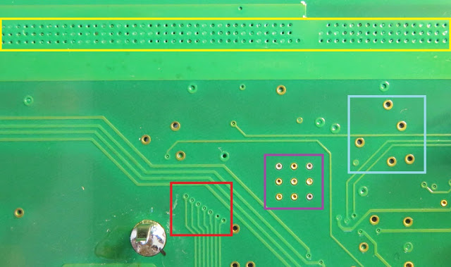
Board outline :
Board outline is the overall shape of the PCB. Generally PCBs are Rectangular shaped but it can be circular, square or any unusual shape based on designers choice and the project need. This feature also marks the size of the PCB board you intend to design.
Layer :
If you have noticed a PCB board you would have noticed the tracks and components on it. The surface on which these tracks and components are placed are called as layers. PCB’s can be single layered or multi layered. The two layer PCB are mostly used but it can go 4 or 8 layer as well. Imagine PCB’s are like a Sandwich several layers are stacked together. For PCB’s which has more than 2 layers, they are constructed in such a way each layer is sandwiched between the top and bottom layer with copper tracks running on it. How they will connect with the bottom and top layer ? You will find the answer when you read about “Via”. The components however can be placed only on either top or bottom side of the PCB. The inner layers are used only for establishing electrical connections. More the number of layer gets complex the PCB gets to design and build.
Track :
While making a circuit on a breadboard or perfboard we generally use wires to connect different components. But in PCB tracks or traces carries the current/ signal between components. As you can imagine complex a PCB board is more number of tracks needed to cover the complete functionality of a board. In complex board copper tracks will be laid on different layers and connected to respective components on the board.
Routing width :
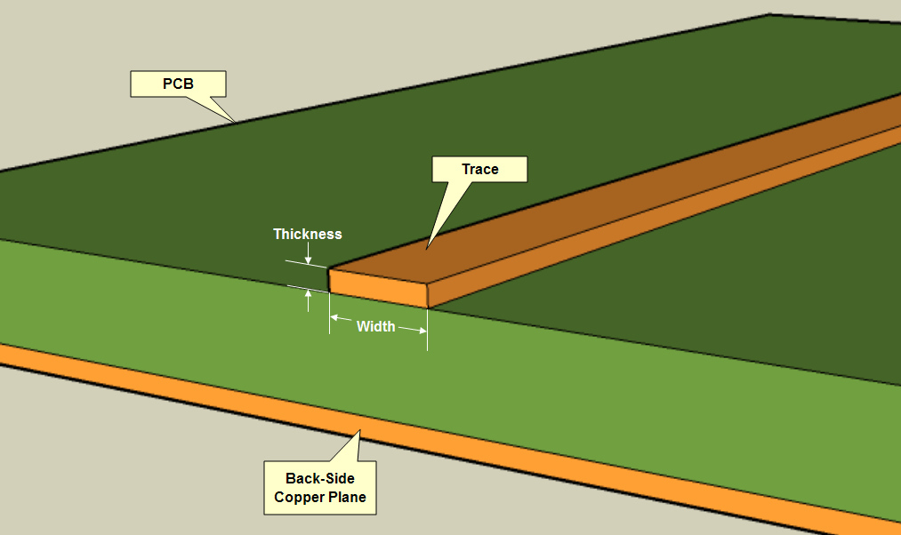
Routing width implies the width of the tracks. Appropriate track width is very important factor when designing PCB’s, specially for those circuits which works on Higher voltage or current. Correct thickness of copper traces ensures safe current transfer and protects the board from overheating issues. High current tracks need to be designed with higher width and for high speed signals Track width and length should be minimum.
This is a very good website to calculate track widths : Routing width Calculator
Via :
Via is conductive pad which connects components or copper area from one layer to another. It is very much used in multi layer PCB boards when we need to connect a track from top layer to a track sitting on the bottom layer. Via can also make this connection possible for more than two layers. Via greatly helps to reduce routing complexity for PCB board and improves efficiency of a board.
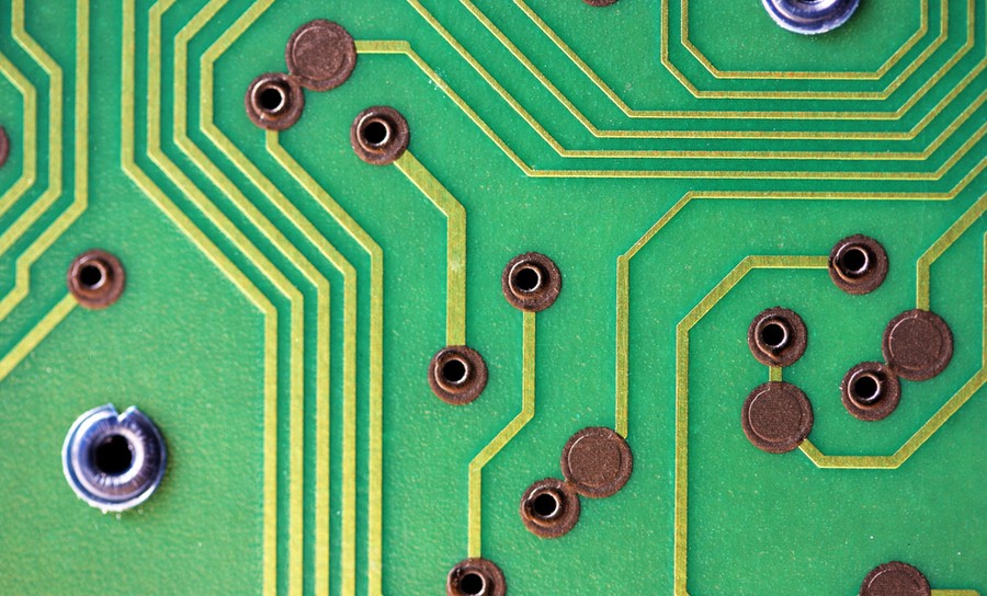
Copper Area :
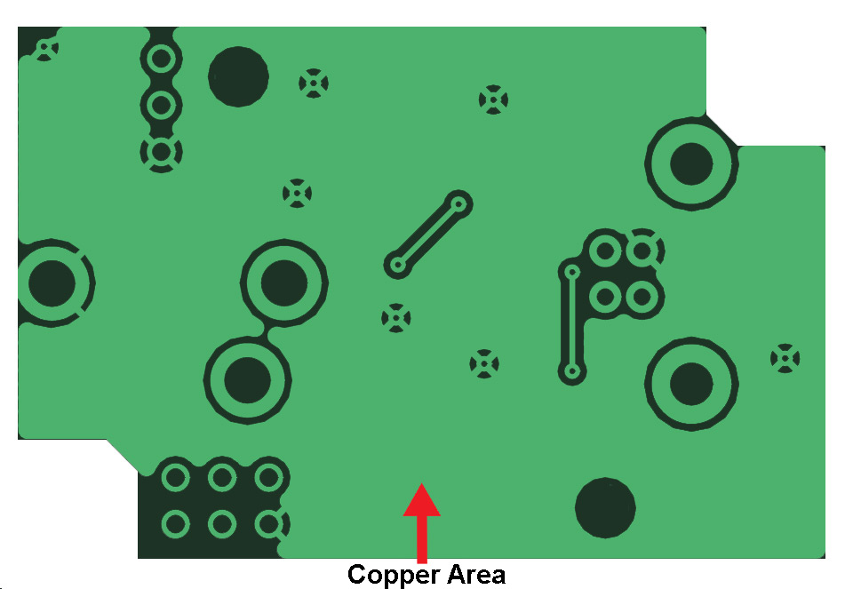
This refers to the unused spaces in a layer of PCB surrounding the tracks etc. This unused area is usually filled with copper pour. This will be particularly handy to make a connection plane for pins/ signals that has multiple connections. In a PCB often there will be many ground points. Instead of joining them manually designers fill the whole area with copper so that it can be a common ground plane that connects all of these points. Apart from making the PCB less messy Ground plane also helps to reduce overall circuit noise and sometimes acts as heat absorbent. There are also instances where Signal planes are formed using this copper area to connect different signal points.
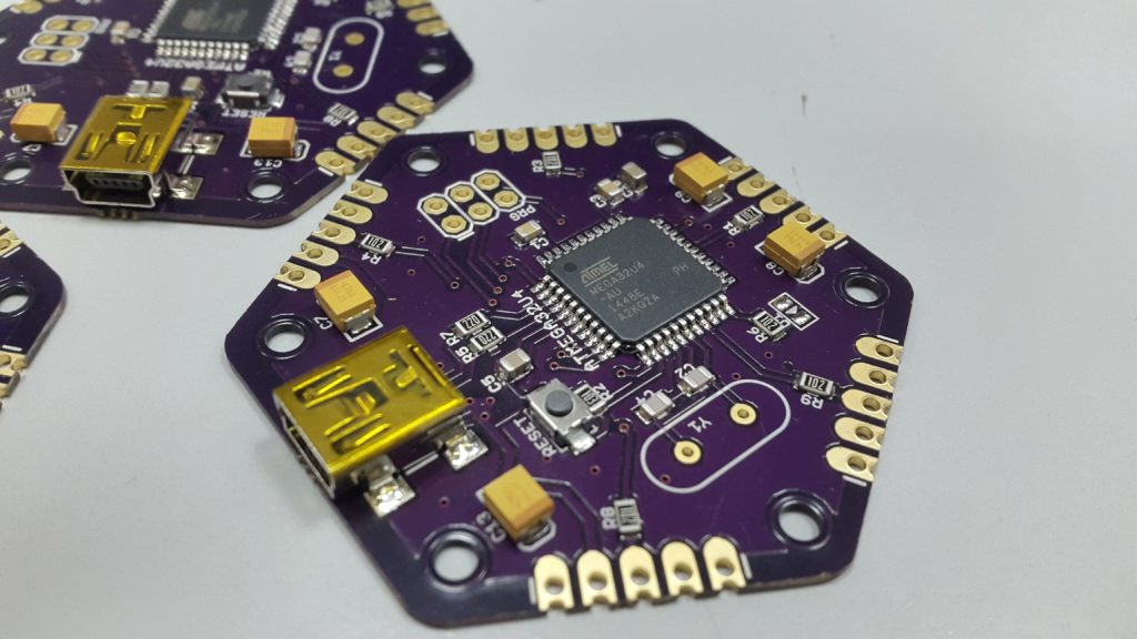
Footprint :
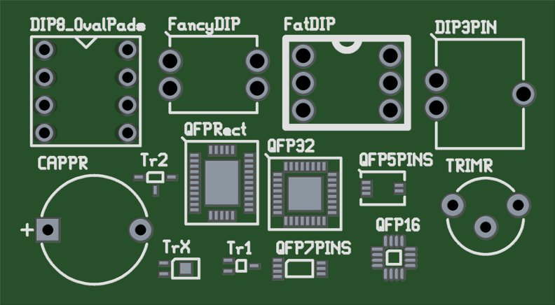
Image courtesy: www.electronics-lab.com
The footprint are conductive pads on PCB where any component sits on. Be it a SMT(Surface Mount Technology) or THT(Through Hole Technology) component they have footprint on which the components can be placed and soldered to the board. The footprints for SMD components will be located on one side of the PCB while THT footprints lies on both sides. Component manufacturers adopt standard PCB footprints while manufacturing their parts to make the PCB designing process feasible and efficient.
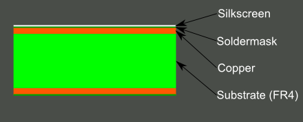
Solder mask :
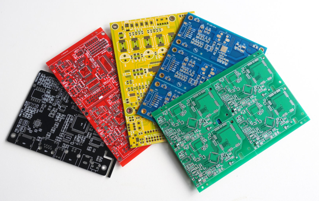
Solder mask is a layer of protective coating applied to PCB. This is mainly used to protect the copper traces from Oxidation. The Soldermask only leaves the component pads uncovered. Additionally this will help the soldering process by preventing the solder from flowing out of the pads to create bridges and short circuit . Solder mask provides aesthetics to manufactured board as this is the reason behind different colors of PCB. Out of which Green solder mask is most commonly used.
Silkscreen :
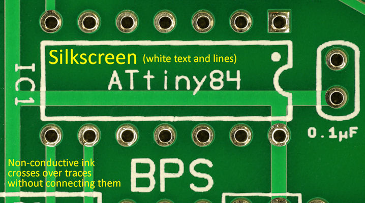
Silkscreen has nothing to do with the actual functionality of the circuit but it is quite useful to provide necessary information about PCB. The necessary information includes component labels, pin location, pad names, company name, logo, graphics or any custom text intended by the designer.
Design rules :
The design rules not a feature in PCB itself but it is related to software part of PCB designing. This is commonly known as DRC and used by many popular design software now . These rules are set using manufacturing factory standards and design should be within the rule. This DRC will check the design and apply the rule so designer mistakes can be detected before sending the design to production.
Gerber files :
These are a group of files that will instruct the PCB manufacturing machine how to build the PCB and what are the characteristics of that particular PCB. After completing the design the designer needs to generate a series of files which contains all the necessary information about every detail in a PCB board. This will be sent to the manufacturer for production.
Bom :
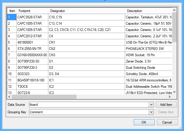
Bill Of Materials or BOM in short contains a list of the components with their part name that are needed to assemble a PCB board. This can be generated from the PCB designing software.
Hope this article was informative to you. We would like to update this list to add more terms that a beginner should be familiar with regarding PCB’s. If you feel we have missed any important terminology in the article, kindly let us know using the comment box below. Feel free to express your thoughts, ask your questions in the comment box as well.


