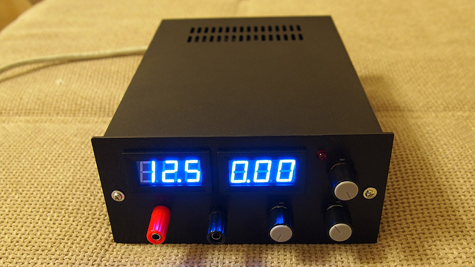
Every lab needs to be equipped with essential equipment. Out of all I would say power supply is most important since it powers up the projects. Batteries, DC adapters can do fine job but as demand grows and project gets bigger a professional and adjustable power supply becomes a necessity. To cater that I have designed an adjustable 50V / 5A power supply with a variable output from 0V to 50V and adjustable current limiting from 0A to 5A. Most simple power supplies cant get the output to come down to exactly 0V or 0A. But in this circuit, the differential amplifiers have a negative power supply rail at (-3V), which can pull the output down to exactly zero.
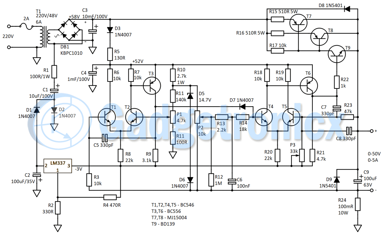
CIRCUIT DIAGRAM OF BENCH POWER SUPPLY:
WORKING:
The power supply relies upon two differential amplifiers made out of Transistors T1 to T6. The first one being responsible for controlling the output current limiting. The second differential amplifier controls the output voltage. They both are driven by the reference voltage created by D5 and D6. The use of zener and a normal diode is to compensate for thermal drift of reference voltage generator. This is because they both have opposing thermal coefficients.
VOLTAGE CONTROL CIRCUITRY:
The voltage control circuitry is created from Transistors T4,T5 and T6. This works by measuring the differential voltage on base terminals of T4 and T5. One terminal is supplied with reference voltage, and the other terminal with some of the output voltage. The reference voltage created by diodes D5 and D6 is around 15.4V. Hence the differential amplifier must amplify the voltage difference by 3.4 times to match the 50V output. This is done by the voltage divider (R23,P3) connected to the inverting terminal of this differential amplifier, setting the gain to 3.4 times of input signal.
When tweaking the power supply, you must set potentiometer P2 to its upper most level. Then fine tune the maximum output voltage to 50V by P3. Since the current sensing resistor (R24) is in a low side configuration, the differential amplifier must correct for the voltage drop it makes when power supply is loaded. This is why the reference voltage generator is connected to the (-) terminal of the power supply and not ground terminal. By connecting the reference voltage generator in such a way, it allows it to drift up or down by the same amount of voltage the current sensing resistor creates as a voltage drop. Therefore it keeps the output steady through the load.
CURRENT LIMITING CIRCUITRY:
The current limiting circuitry is comprised of Transistors T1,T2 and T3. This works by measuring the voltage drop created by current sensing resistor and comparing it to a given reference voltage created by R11 and P1. I actually suggest replacing R11 with a 220k trimmer and fine tuning the maximum current limit to match your requirements.
As it is, the protection is set to enable at 5.3A. With an adjustable value for R11, you can set the protection at any level up to maybe 6-7A without compensating the circuit for increase in power. When the protection is ON, T3 drops the voltage at its collector, thus creating an appropriate potential difference through the diode D7. At this point it starts stealing some of the biasing voltage of T4. By dropping the base voltage of T4, output voltage drops sufficiently to keep the current through the load constant.
GERBER FILES:
A big thanks to Morne Stander for designing PCB for this circuit and sharing it with the community. You can download the Gerber files below
I hope the author does not mind but I’ve done a PCB design for the project and I don’t mind sharing it. I have however doubled up on the output transistors and have also changed them to TO213 Package devices. I just find them easier to mount instead of the TO3 Package devices.I have also changed the Bridge circuit slightly to make use of a center tapped AC supply, but this can easily be modified for transformers with no center tap.
Hi Morne,
We would love your contribution to this project Morne. Can you kindly forward the PCB design image and gerber files to frankdonald(at)gadgetronicx.com . I will add it here with design credits to you. Thanks in advance.
I’ve finished simulating this circuit with the changes suggested by bernard in the comments. I want to build the pcb for this board next (I want to learn pcb designing). I plan to route all the traces myself but having a copy of your pcb as a guide might be a huge help. could you please send me a copy at kinohermetic@gmail.com?
The problem is power dispation is about 250 watt it need big heat sink and big surface and maybe forced ventilation your transitor will work but they will heat up more then TO3 package if you do so you should use a transformer with multiple output to select the best output to drive the power supply
Hi,
i am quite new to circuit design, so I’m sorry if the following issue is self-evident to the rest of you guys, but I wanted to know if it was possible to set the voltage and current limit with two voltages (without major modifications) e.g. provided by a DAC? I need to drive a solenoid(0.1-1H) with 0-48V and 0-1.5A as ripple-free and linear as possible. I have been searching the internet for quite a while now, but it seems to be a tricky task.
Thank you in advance for your help 🙂
Hello Friend ! Your project seems to be excellent, I have been looking for a project like this for years, I am already assembling the circuit, do you have the layout of the printed circuit board (PCB)? I’m in Brazil. if so, could post, it would be of great use to all of us.
I have a Transoformer 24 0 24v 5amps, and was just looking for a circuit like this, if you can help me with the PCB schematics, I can work towards this project and give you updates. my email ID is patrickvaz2002@gmail.com.
regards
This circuit is very interesting.
I think Bernard is right. Reference and feedback (T4, T5) should have the same reference (P3 to – lead). Otherwise, the voltage drop in R24 won’t be compensated.
C3 is too small, it should be at least 2,200uF.
220V should not be connected to gnd.
I would replace the power transistor T7, T8 with 15A NPN (TIP 135).
R2, R4 should be swapped.
I will add a cc Led.
I intend to build up your schematic in the mirror. LM317>LM337, BD140>BD139, BC547>BC546, BC557>BC556. And ofc every stuff and the negative/positive logic in the mirror. Can I use 2n3055 instead of MJE15004? If I could, the value of shock resistors R15,R16 will be the same like in your schematic (510R)?
And ADJ divisor R2/R4? R4 must be 240 according to the 1.25(1+R2/R3) = 3V, didn’ be? I think is a typing mistake. Tnx.
Hallo I was wondering if you can use NPN transistors instead of PNP
Because I already have build something similar with NPN but still looking for a good schematic to drive them
Hi, I did a lot of simulations. I see that the voltage reference from D4 and D6 are related to the – lead but the feedback form the output is related via R23 and P3 to the -3V (which is a stable voltage), then the voltage drop is not compensated. Change the P3 to the – lead then it is compensated. The differential T4, T5 have then the same references.
Comments?
Hi, with the R4 = 470 ohm it gives about -2.1V, is that used in your pcb supply instead of the 240 ohm as other people suggested (datasheet LM337)?
I see that the -3V (R4= 240 ohm)as ripple that can be reduced by add 1uF capacitor parallel on R2 and 1uF on the -3V, and make the C1 and C2 higher capacitance.
As you suggested, I removed the Cap on the base of T9 (ripple came from -3V). The response is quicker (<2ms in stead of 200ms).
It can be more quicker by reducing the output capacitance 100uF to 22uF (reduce short peak currents), but isn't a big issue.


I hope the author does not mind but I’ve done a PCB design for the project and I don’t mind sharing it. I have however doubled up on the output transistors and have also changed them to TO213 Package devices. I just find them easier to mount instead of the TO3 Package devices.I have also changed the Bridge circuit slightly to make use of a center tapped AC supply, but this can easily be modified for transformers with no center tap.
Hi Morne,
We would love your contribution to this project Morne. Can you kindly forward the PCB design image and gerber files to frankdonald(at)gadgetronicx.com . I will add it here with design credits to you. Thanks in advance.
Great job Morne Stander. could you please share with us ?
tolgagercek(at)yahoo.com
Thank you, that sounds amazing. I would love to tinker with that design, too! Could you send it to incaseofzombiesuseportals(at)gmail.com ?
Thanks 🙂
Hi Morne, Can you send the pcb design to arkamaity007.s@gmail.com?
Hi, can you send me the PCB design at michele.baffari@gmail.com ? Thank you.
Hello, good day.
I’ve finished simulating this circuit with the changes suggested by bernard in the comments. I want to build the pcb for this board next (I want to learn pcb designing). I plan to route all the traces myself but having a copy of your pcb as a guide might be a huge help. could you please send me a copy at kinohermetic@gmail.com?
The problem is power dispation is about 250 watt it need big heat sink and big surface and maybe forced ventilation your transitor will work but they will heat up more then TO3 package if you do so you should use a transformer with multiple output to select the best output to drive the power supply
Would you plse share pcb design? thanks in advance…
hi, i have some interesting circuit that you might like, message me to my email ion.marius.dorinel@gmail.com if interested
Hello R15,16 510ohm ??? correct
No must be 0.5ohm 5Watt
Yess…Probably not 510R.. more like R510
Hi,
i am quite new to circuit design, so I’m sorry if the following issue is self-evident to the rest of you guys, but I wanted to know if it was possible to set the voltage and current limit with two voltages (without major modifications) e.g. provided by a DAC? I need to drive a solenoid(0.1-1H) with 0-48V and 0-1.5A as ripple-free and linear as possible. I have been searching the internet for quite a while now, but it seems to be a tricky task.
Thank you in advance for your help 🙂
Hello Friend ! Your project seems to be excellent, I have been looking for a project like this for years, I am already assembling the circuit, do you have the layout of the printed circuit board (PCB)? I’m in Brazil. if so, could post, it would be of great use to all of us.
Hi Arruda,
Unfortunately we don’t have a PCB for this project.
Hi Frank. I’ve done the PCB design for it and if the author does not mind I will share it online. I’m just not sure how to upload it on here.
hi sir can you share pcb design and modified schematics with me ..email shaingsm @gmail.com
Dear Mr. Stander,
I have a Transoformer 24 0 24v 5amps, and was just looking for a circuit like this, if you can help me with the PCB schematics, I can work towards this project and give you updates. my email ID is patrickvaz2002@gmail.com.
regards
PS:Thank you Mr. Damyanov
This circuit is very interesting.
I think Bernard is right. Reference and feedback (T4, T5) should have the same reference (P3 to – lead). Otherwise, the voltage drop in R24 won’t be compensated.
C3 is too small, it should be at least 2,200uF.
220V should not be connected to gnd.
I would replace the power transistor T7, T8 with 15A NPN (TIP 135).
R2, R4 should be swapped.
I will add a cc Led.
C3 10mF = 10000uF
I intend to build up your schematic in the mirror. LM317>LM337, BD140>BD139, BC547>BC546, BC557>BC556. And ofc every stuff and the negative/positive logic in the mirror. Can I use 2n3055 instead of MJE15004? If I could, the value of shock resistors R15,R16 will be the same like in your schematic (510R)?
And ADJ divisor R2/R4? R4 must be 240 according to the 1.25(1+R2/R3) = 3V, didn’ be? I think is a typing mistake. Tnx.
Hallo I was wondering if you can use NPN transistors instead of PNP
Because I already have build something similar with NPN but still looking for a good schematic to drive them
220v is connected to ground?
Hi, I did a lot of simulations. I see that the voltage reference from D4 and D6 are related to the – lead but the feedback form the output is related via R23 and P3 to the -3V (which is a stable voltage), then the voltage drop is not compensated. Change the P3 to the – lead then it is compensated. The differential T4, T5 have then the same references.
Comments?
Hi, with the R4 = 470 ohm it gives about -2.1V, is that used in your pcb supply instead of the 240 ohm as other people suggested (datasheet LM337)?
I see that the -3V (R4= 240 ohm)as ripple that can be reduced by add 1uF capacitor parallel on R2 and 1uF on the -3V, and make the C1 and C2 higher capacitance.
As you suggested, I removed the Cap on the base of T9 (ripple came from -3V). The response is quicker (<2ms in stead of 200ms).
It can be more quicker by reducing the output capacitance 100uF to 22uF (reduce short peak currents), but isn't a big issue.