
If you are making a hardware project that requires a microcontroller, don’t just go for MCU that’s lying around. Choose Microcontroller that’s fit for the job. Don’t go for a 32 bit MCU when all you need to do is take input from a sensor. In this tutorial we are going to discuss ATtiny85 which is a good thing that comes in small package. This microcontroller is loaded with functionality but comes in a small package as DIP8 thus enabling you to reduce your board size still offering great performance.
As a beginner tutorial we will make a LED blink using ATtiny85 Micrcontroller. This tutorial will cover
- Features of ATtiny85
- Core registers used in configuring ATtiny85 microcontroller
ATtiny85 :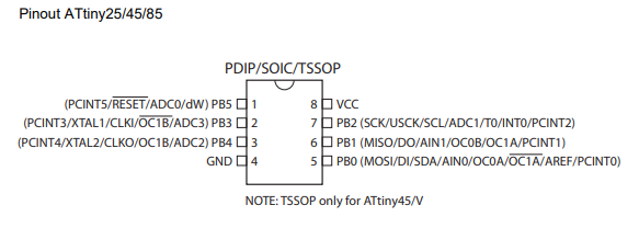
It is based on Atmel Attiny85 MCU. Talking about the size this is almost 1/3 of the size of an Arduino nano but offers quite a few specs as compared to Arduino uno. ATtiny85 is a 8 pin IC out of which 6 pins are GPIO pins, 2 power pins. And unlike Atmega328p IC it doesn’t require any extra passive components to function. Specifications of ATtiny85 includes
- 6 I/O pins
- Timers
- Counters
- Compare match
- PWM on 3 pins (P0, P1 and P4)
- ADC on 4 pins (P2 to P5)
- Analog comparator
- External Interrupt on pin P2
- SPI protocol
- I2C protocol
- Sleep modes
You can look into its datasheet to know more about this IC.
The datasheet of ATtiny85 shows there are three registers involved in order to use any GPIO pin in ATtiny85. In our tutorial we intend to use PB1 as output let’s see what are these registers and how to configure them to make PB5 as output.
DDRB register:
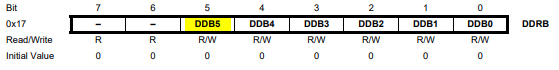
This is the first register that need to be configured to use PB5 pin as GPIO. As you can see in the above register diagram, you can observe there are 5 readable as well as writeable bits in this register. Each one of these bits DDB1, DDB2…DDB5 controls the direction of physical pins PB1, PB2 ….PB5. Writing “1” to these pins will configure the GPIO pin as output and “0” will configure it as input. In our case we need to configure PB5 as output, therefore we need to write the DDB5 bit as logic “1” through code. This register is port addressable so to write 1 in DDB5 we use DDRB=0b00100000
PORTB register:
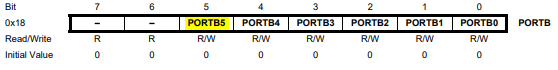
Now that we have set our PB5 pin as output we can proceed to next step. This PORTB register is used to toggle the output state of pins in our controller. Similar to DDRB register each bit is responsible for output of pins PB1…PB5. Our point of interest is PB5 pin therefore to make PB5 output high we write PORTB5 logic “1” and logic “0” when we need PB5 to turn low. So to make a blinker we need to write logic 0 and logic 1 alternatively with specific time delay in PORTB5 of this register. This is port addressable where to toggle PB5 to output you need to write PORTB=0b00100000.
PINB register:
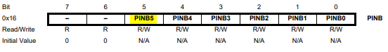
The structure of this register is quite similar to the above two registers. PINB1 to PINB5 responsible for output of PB1 to PB5. You might ask why there are two registers to control output of PORTB pins. This register is bit addressable meaning you can address any single bit in this register and toggle its value without disturbing its other bits whereas above two registers are PORT or byte addressable where you cannot instruct a single bit individually. So here if you need to activate PB5 you can simply instruct the bit PINB5=1 in the above register. This value will toggle the corresponding bit of PORTB register automatically.
Programming ATtiny85
To get started with ATtiny85 it is advised to use Digispark ATtiny85 development board. It is plug and play development board with on board LED for easier debugging. Alternatively you can program ATtiny85 by configuring Arduino or other development boards as ISP.
Follow the instructions provided in this article to setup your Digispark ATtiny85 board with Arduino IDE or Program ATtiny85 using Arduino as ISP
Code:
#include<avr/io.h>

void setup()
{
  DDRB |=(1 << DDB5);  //set PB5 as output
}

void loop() {

   PORTB |= (1 << PB5);    // Turning ON LED connected to PB1
   delay(1000);            //Using Arduino IDE inbuilt delay function to generate delay of 1 second
   PORTB &= ~(1 << PB5);   //Turning the LED off
   delay(1000);
}
Try this out:
- Set direction of pins PB0, PB1 and PB2 as output. Toggle pins PB0, PB1, PB2 with time delay of 500ms, 1000ms and 1500ms.
Other tutorials:
- ATtiny85 GPIO as input
- ATtiny85 timer to create time delays
- ATtiny85 as counter to count events or signals
- ATtiny85 compare match


Hello.
Excelent tutorial series. Helped me a lot to clarify some code and registers.
I was wondering if you are planning something like these for the “New” AtTiny1614.
I was looking for some information about interrupts, GPIO, all the works, but sadly there´s not enough info.
Thank you again for your time and effort.
Orlando.