
Following the series of ATtiny85 tutorials this article explains how to configure ADC in an ATtiny85 microcontroller. Analog to digital converter aka ADC is quite an important feature in microcontrollers where it will translate the Analog signals to digital data. This is most commonly used with sensors to measure parameters from operating environment and enable microcontroller to interpret the environmental conditions.
Analog to Digital Converter ( ADC ) in ATtiny85:
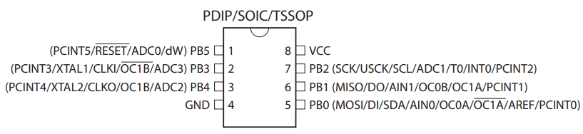
There are total of 4 ADC channels present in ATtiny85. These channels are interface to to pins PB2, PB3, PB4, PB5 in port B. Also ATtiny85 ADC is of 10 bit resolution. Meaning the input Analog signal can be translated to 10 bit data. The maximum analog input voltage to this microcontroller can range from 0V to 5V.
Let’s look into the configuration of this ADC in ATtiny85 controller.
ADMUX – ADC Multiplexer Selection Register:
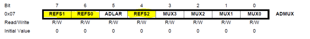
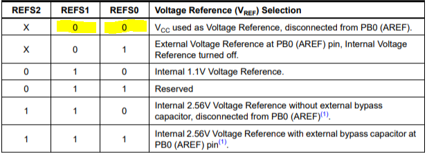
ADMUX register should be used to configure ADC peripheral in ATtiny85. REFS0, REFS1, REFS2 bits are used to select reference voltage used with ADC. We are using Vcc as reference voltage hence used the values 0,0,0.
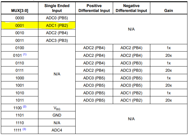
MUX0, MUX1, MUX2, MUX3 bits are used to select the ADC channel which the user intended to use. We have selected ADC1 to use for our tutorial purposes hence we write 0001 to MUX[3:0].
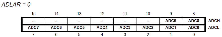
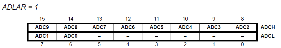
Finally the ADLAR is used to define how the resultant translated digital data should be stored in the register. There are two data registers associated with ADC, these are ADCL and ADCH. The final result after ADC conversion is stored in these two data registers. Each register has a maximum of 8 bits. Since our ADC resolution is 10 bits, the data will be split into two and stored into ADCL and ADCH register.
If ADLAR is set to 0, 8 bits of converted data will be stored in ADCL and 2 bits in ADCH. This is known as right shifted result.
If ADLAR is set to 1, 8 bits of converted data will be stored in ADCH and 2 bits in ADCL. This is known as left shifted result.
ADCSRA – ADC Control and Status Register
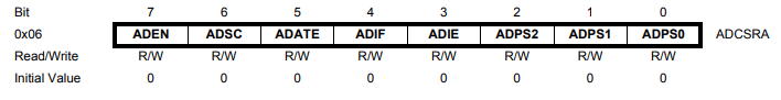
ADEN is ADC enable bit which has to be set to 1 to enable ADC feature.
ADSC: ADC Start Conversion bit starts the conversion when set to 1. After ADC conversion is performed this bit will be set back to zero by hardware.
ADATE: Enabling this bit enables the auto triggering of ADC conversion. This conversion occurs every positive edge of trigger ( discussed below ) and continues to repeat after each conversion as long as the trigger signal is intact. The converted values from ADCH and ADCL has to be read before the next conversion replaces the current result.
ADIF: ADC Interrupt Flag, this will be set to 1 by hardware when ADC conversion completes. The ADC interrupt will be be executed when ADIF goes high if you choose to enable the ADC interrupt using ADIE bit. ADIF bit will be cleared by the hardware when that particular service routine is executing.
ADIE: ADC Interrupt Enable – When this bit is set 1 and global interrupt enable bit I in SREG register is set then ADC conversion triggers interrupt.
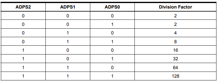
Bits ADPS2, ADPS1 and ADPS0 are the prescaler selection bits to divide the clock frequency at which ADC operates. The below table shows the values in these bits and their respective divisible factor. Setting these bits to 111 will choose the divisible factor of 128 which sets the ADC to operate at lowest operating frequency.
ADCSRB register:
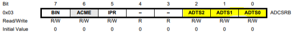 ADTS0, ADTS1 and ADTS2 bits in ADCSRB register decides when ADC conversion will be triggered. Below table shows the various trigger sources for the ADC conversion. The ADATE in ADCSRA bit has to high in order for these trigger sources to take effect.
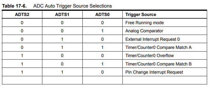 When you select the free running mode. Conversion repeats over and over again until it is stopped. In this free running mode the interrupt will not be triggered even when the ADC interrupt flag ADIF flag is set.
Other trigger sources doesn’t fall under above category. For example when these bits are written 100, then ADC will be triggered when Timer/ Counter0 overflows. This will set the ADIF flag and ISR will be executed if ADC interrupt is configured.
ADC conversion:
The ADC conversion result for the single ended conversion can be calculated with the formula
ADC = ( Vin x 1024 ) / Vref
So, for this tutorial, we have chose Vref is 5V. Let’s say a sensor that we use with outputs a voltage of 2.46V, then ADC converted value will be
ADC = Vin * 1024 / Vref
= 2.46 * 1024 / 5 = 2519.04 / 5
= 503.80
This value will be stored in binary form in both ADCH and ADCL register when 10 bit resolution is selected.
SREG- AVR Status Register

As stated earlier interrupts can be used with ADC. This will be triggered at the end of each ADC conversion. In order to use this conversion, Bit I of SREG register which is global interrupt enable bit should be written as 1. This should be followed by enabling ADIE bit ADCSRA register.
Circuit diagram:
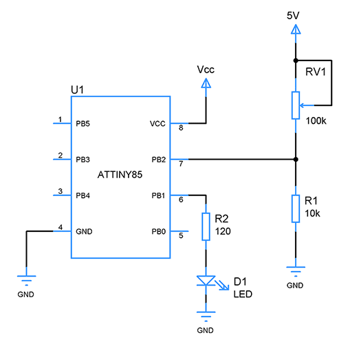 Potentiometer RV1 connects to PB2 to feed analog signal. PB1 connects to LED which serves as an indicator for predefined analog input ranges.
Sample Code for ADC in free running mode :
Code to read Analog signal from potentiometer connected to PB2 and light up or toggle LED connected to PB1 based on the analog voltage.
#include<avr/io.h>
#define F_CPU 16500000UL

void adc_setup()
{
 DDRB|=(1<<PB1);         //PB1 as output to activate LED
 ADCSRA|=(1<<ADEN);      //Enable ADC module
 ADMUX=0x01; // configuring PB2 to take input
 ADCSRB=0x00;           //Configuring free running mode
 ADCSRA|=(1<<ADSC)|(1<<ADATE);   //Start ADC conversion and enabling Auto trigger
 }

int main()
{
 adc_setup();
 while(1)
 {
 int adc_l=ADCL; //value of Input  Voltage in lower register
 int adc_val=(ADCH<<8)|adc_l;   //Reading ADCH and coimbining the data
 if (adc_val>=510&&adc_val<=520) //Lights up the LED under certain voltage 2.25 to 2.3 level
  {
   PORTB|=(1<<PB1);  //LED remain ON
  }

 else        //blink condition
  {
    PORTB &=~(1<<PB1); //LED toggle
  }
 ADCSRA|=(1<<ADIF);
 }
}
Sample Code for ADC with Timer0 overflow trigger:
Code to read Analog signal from potentiometer connected to PB2 and light up LED in PB1 by means of Timer0 value overflow as trigger.
#include<avr/io.h>
#define F_CPU 16500000UL

void adc_setup()
{
 DDRB|=(1<<PB1);
 TCCR0A=0x00;             //Timer0 normal mode
 TCCR0B=0x00;
 TCCR0B |= (1<<CS00)|(1<<CS02);   //prescaling with 1024
 TCNT0=0;
 ADCSRA|=(1<<ADEN);       //Enable ADC module
 ADMUX=0x01; // configuring PB2 to take input
 ADCSRB|=1<<ADTS2;   //Timer / Counter 0 overflow triggers the ADC to perform conversion
 ADCSRA|=(1<<ADSC)|(1<<ADATE); //Enabling start of conversion and Auto trigger
 }

int main()
{
 adc_setup();
 while(1)
 {
 int adc_l=ADCL;   //value of Input  Voltage
 int adc_val=(ADCH<<8)|adc_l;   //Storing entire ADC value in a variable
 if (adc_val>=510&&adc_val<=520) //Trigger the ADC when the voltage value falls within 2.25 to 2.3v
  {
   PORTB|=(1<<PB1);
  }

 else  //blink condition
  {
    PORTB &=~(1<<PB1); //Toggle LED state
  }
 TIFR|=(1<<TOV0);  //Clearing overflow flag
 }
}
Try this out:
- Configure two ADC channels ADC1 & ADC2 to run in free running mode, read the ADC values and update it in a variable every 10 seconds.
Other ATtiny85 tutorials:
- ATtiny85 Analog comparator tutorial
- ATtiny85 External and Pin change interrupt tutorial
- ATtiny85 sleep modes
- ATtiny85 PWM: Fast and Phase correct modes


