I2C or Inter Integrated circuit is another popular serial communication protocol built in almost every modern microcontrollers. This protocol uses full duplex communication and uses only two wires to exchange data. ATtin85 microcontroller is equipped with Universal Serial interface aka USI which can be configured to operate in I2C mode. I2C mode using this USI interface is also referred as Two wire mode. In this tutorial we will see how to configure USI as I2C protocol in ATtiny85 microcontroller to send and receive data between devices.
ATtiny85 I2C protocol or Two wire mode:
I2C is a popular serial communication protocol where the data bits transmission takes place via two wires – SDA and SCL. SDA is the data line in which the data bits are transmitted and received. I2C is a half duplex communication since there is one data line. SCL is the clock signal line which is used to synchronize the communication. Similar to SPI communication, I2C protocol establishes communication by assigning devices as Master and Slave. The device which generates clock signal will be the master device. But unlike SPI protocol which uses a dedicated pin SS to select slave device for communication. I2C protocol uses slave address for selecting the slave which master wishes to communicate.
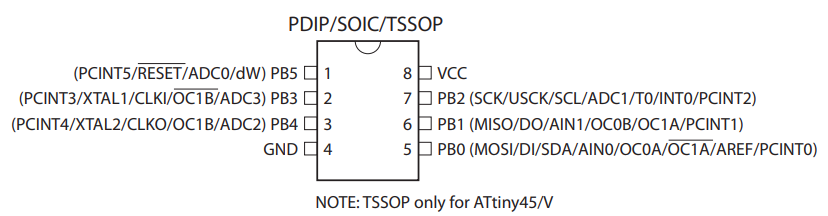
When master need to communicate it will send slave address via data line SDA. The slaves connected to master will receive the address. And then only the slave matching the address will store the incoming data from master device and other slaves will discard the incoming data from master. In ATtiny85 microcontroller SDA pin is PB0 and SCL pin is PB2. Read more about this protocol in detail.
A – In ATtiny85 this start condition occurs when master device pulls the SDA line low while keeping the SCL line high. This can be done by writing the PB0 pin to zero or low. Now the start detector of the slave device deduces this as start condition and sets the USISIF flag.
B – In response to the start condition the start detector of the slave device pulls the SCL line low. This will help slave to be prepared to receive the slave address from Master device. Once the slave is prepared to receive the address, it clears the USISIF flag.
C – The Master device now set the first bit of address to be transmitted and pulls the SCL line high again. Now the address is transmitted followed by Read / Write bit via SDA with synchronizing clock in SCL.
D – When the address didn’t match the slave’s device address, the slave releases the SCL. However if slave address matches with the address received, the SDA line is pulled low by the slave while acknowledgement pulse is in progress. Depending on read or write operation either Master or Slave device will take control of SDA line.
E – After taking control of SDA line the data bytes can be transmitted with each byte transmission followed by a acknowledgement biy. This will continue until Master device issues stop condition by pulling the SDA line high after a positive edge in SCK pin.
F – Stop condition occurs where the SCL line is pulled high first and then SDA line is pulled high with a considerable delay between each transitions.
USICR register:
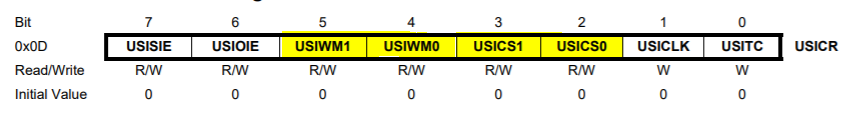
This is the register that is used to set the USI interface to operate in I2C mode. The bits USIWM1 and USIWM0 need to set 0 and 1 to configure the ATtiny85 in two wire or I2C mode. USICS0, USICS1 and USICLK bits are used to select the clock that will be used for I2C communication. The below table shows the various clock sources that can be used for our I2C communication and clock to power a 4 bit counter which is responsible for keeping the track of data sent or received. We choose USICS1 and USICLK bits are set to 1 to select the respective modes.
The synchronizing clock from SCL pin for this communication can be generated using USITC bit. The SCL pin state toggles from high to low and from low to high every time 1 is written to USITC bit.
USIDR register:
This the actual register which holds the data that need to be sent and the data that is received from other devices. User need to write 8 bit data in this register and then transmit the data by activating clock pulses to synchronize the transfer. Similarly when the ATtiny85 receives the data each bit received and placed in the USIDR register. When transfer of a byte is complete, data in USIDR register will be copied to USIBR register.
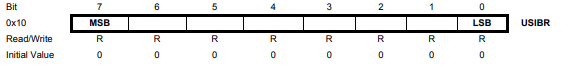
USIBR register:
This is the similar to the USI data register. Contents of USIDR register will be copied to USI Buffer register when data transfer is complete. This provides user with time to read the data when the data transfer is time sensitive.
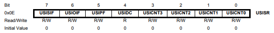
USISR register:
USISR register bits with holds the status of the I2C communication. Each bits will reveal different status of the ongoing communication
USISIF: This bit goes high when there is a start condition detected in I2C communication
USIOIF: This bit goes goes high when the clock counter overflows, this is used to indicate whether a particular data byte has been transmitted or received.
USIPF: This bit goes high when the stop condition is detected in I2C communication.
USIDC: This bit indicates where there is a data collision that can occur when multiple masters are used in I2C communication.
USICNT3, USICNT2, USICNT1, USICNT0: These 4 bits holds the counter value that keeps track of the data bits that has been transmitted or received between devices in I2C communication.
Circuit diagram for I2C communication:
Steps to configure ATtiny85 to use I2C protocol and send data as Master:
Configure the USI to operate in Two wire interface or I2C mode using USICR register.
Use the data direction register DDRB to set pins PB2 (SCL) and PB0 (SDA) as output.
Initiate start condition by pulling the pins SCL and SDA low
Wait until the start condition flag USISIF flag is set.
Write the 7 bit address of slave along with read “1” or write “0” into USIDR register.
Generate clock signal in SCL pin by writing one to USITC bit and wait for SCL to go high
Toggle the USITC bit again with considerable delay to force SCL go low.
Repeat the clock generation until the USIOIF flag overflows which indicates the byte is transferred
Change the direction of SDA pin to low to receive acknowledge bit
Load the USICNTx counter with 1110 so that the counter overflows after receiving 1 ack bit.
Read the USIDR register to see if the ack bit is 1
Send the actual data now using the steps 6,7 and 8.
Sample code for configuring ATtiny85 as master and send data:
#include<avr/io.h>
String tosend="test";
//PB2 -SCL
//PB0 - SDA

void i2c_ack()
{
  DDRB&=~(1<<PB0);  //Change direction of SDA to receive acknowledge bit
  USISR|=(1<<USICNT3)|(1<<USICNT2)|(1<<USICNT1); //Set counter to 1110 to force it to overflow when ACK bit is received
  i2c_transfer();   //Byte transmission
}

void i2c_transfer()
{
  do
  {
  USICR|=(1<<USITC);   //Clock signal from SCL
  while((PINB&(1<<PB2))); //Waiting for SCL to go high
  delayMicroseconds(5);
  USICR|=(1<<USITC);  //Toggle SCL to go low
  delayMicroseconds(5);
  }while(!(USISR&(1<<USIOIF)));  //Repeat clock generation at SCL until the counter overflows and a byte is transferred
  delayMicroseconds(5);
  USISR|=(1<<USIOIF);      //Clear overflow flag
}

void i2c_actual_data()
{
  DDRB|=(1<<PB0);
  short int i=0;
  while(tosend[i]!='\0')  //Actual data string "test"
  {
    USIDR=tosend[i];     //Placing byte in Data register
    i2c_transfer();      //Transfer the data placed in register
    i++;
  }
}

void i2c_start()
{
  PORTB&=~(1<<PB0);  //Pulling SDA line low
  delayMicroseconds(5);
  PORTB&=~(1<<PB2);  //Pulling SLC line low
  delayMicroseconds(5);
  while(USISIF==1); //detection of start condition
}

void initialize()
{
  USICR=(1<<USIWM1)|(1<<USICS1)|(1<<USICLK);  //TWI mode
  DDRB=(1<<PB0)|(1<<PB2); //SDA & SCL direction as output
  PORTB=(1<<PB0)|(1<<PB2); //SDA & SCL default state
  i2c_start();
  USIDR=0b00000000; //address of slave and select write operation
  i2c_transfer();
  i2c_ack();
}

void i2c_stop()
{
  PORTB|=(1<<PB2);       //Pulling SDA high
  delayMicroseconds(5);
  PORTB|=(1<<PB0);       //Pulling SCL low
  delayMicroseconds(5);
}

int main()
{
 initialize();      //initialize i2c
 char usi_data;
 usi_data=USIDR;
 if(usi_data&0x01)
 i2c_actual_data();  //transmit data
 i2c_stop();         //i2c stop
 return 0;
}
Steps to configure ATtiny85 to use I2C protocol and send data as Master:
Configure the USI to operate in Two wire interface or I2C mode using USICR register.
Use the data direction register DDRB to set pins PB2 (SCL) and PB0 (SDA) as input.
Set counter to zero.
Wait for the counter overflow flag USIOIF to one.
Check the slave address received in the USIDR register.
If the address matches the slave address send the acknowledge bit to the master
Clear the counter.
Wait for the overflow flag USIOIF bit to be set to one.
Once it is set to one, a byte is successfully received in the USIDR register.
Read the USIDR register to retrieve the data sent from the master device.
Repeat the step 8,9 and 10 to receive further data from master device.
Sample code for configuring ATtiny85 as slave and receive data:
#include<avr/io.h>
String received;
//PB2 - SCL
//PB0 - SDA
short int flag;
short int i=0;

void initialize()
{
  USICR=(1<<USIWM1)|(1<<USICS1)|(1<<USICLK);  //TWI mode
  DDRB=0x00; //SDA & SCL direction as input
  PORTB=0x00; //SDA & SCL default state
  USISR=0x00;       //Counter value
}

void i2c_address()
{
  char usi_data;
  while(USISIF==0);    //Wait till address bit is received
  {
    usi_data=USIDR;
    if(usi_data==0x00)  //Verifying the address
    {
      i2c_ack();   //Send acknowledge bit
      flag=1;
    }
  }
}

void i2c_ack()
{
  DDRB|=(1<<PB0);       //Set the direction to output
  USISR|=(1<<USIOIF);   //clear overflow flags
  PORTB|=(1<<PB0);
  while((USISR&0x01)==0); //Wait until counter goes 1
  PORTB&=~(1<<PB0);     //Ack bit end
  USISR&=0xF0;          //Clear counter bits
}

void receive_data()
{
  if((flag==1)&&(USIOIF==1))    //Checked address and counter overflow bits
  {
    received[i]=USIDR;   //Received data stored in string
    i++;
    USISR|=(1<<USIOIF);  //Clear overflow flag
  }
}

int main()
{
  initialize();      //i2c configuration
  i2c_address();     //check address
  i2c_ack();         //acknowledge bit
  while(1)
  {
   receive_data();   //receive data and storing data
  }
}
Try this out:
Set up two ATtiny85 with one being master and other being slave.
Write code for both Master and Slave device.
Master device should send a string “Hi” and Slave responding back “Ok” upon successfully receiving the data.
Hi, Thank you for this project.
I have a question. How can I do 10-bit addressing. I want 1000 Slave cards and 1 master card. I use ATtiny85 chip for slave cards. And I use ATSAM3X8e for master card.
Thanks for getting this code all in one place. Much of it looks accurate. However, I’ve noticed something.
while(USISIF==0); //Wait till address bit is received
That line is doing nothing. USISIF is a bit position number. According to the ATTIny85 datasheet it should equal 7. It is a constant and its value will never change. So that while loop will fall through immediately.
Further, although this is only slightly more than a knit-pick, the arrangement of a code block ({ … }) underneath it makes for a misleading code-read. The while condition’s code is actually a semi-colon no-op. The block is just a list of top-down code.
Hi, This article is very informative. Currently i’m looking for AtTiny 402 interfacing with RTC via I2C protocol. If you have AtTiny 402 I2C example code then it will helpful for me.

 I2C is a popular serial communication protocol where the data bits transmission takes place via two wires – SDA and SCL. SDA is the data line in which the data bits are transmitted and received. I2C is a half duplex communication since there is one data line. SCL is the clock signal line which is used to synchronize the communication. Similar to SPI communication, I2C protocol establishes communication by assigning devices as Master and Slave. The device which generates clock signal will be the master device. But unlike SPI protocol which uses a dedicated pin SS to select slave device for communication. I2C protocol uses slave address for selecting the slave which master wishes to communicate.
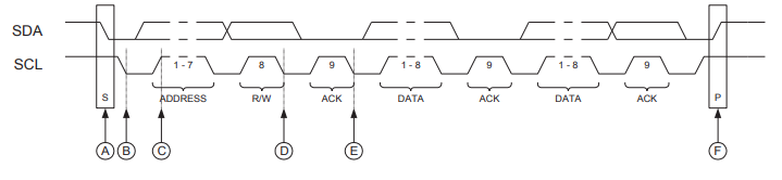
 This is the register that is used to set the USI interface to operate in I2C mode. The bits USIWM1 and USIWM0 need to set 0 and 1 to configure the ATtiny85 in two wire or I2C mode. USICS0, USICS1 and USICLK bits are used to select the clock that will be used for I2C communication. The below table shows the various clock sources that can be used for our I2C communication and clock to power a 4 bit counter which is responsible for keeping the track of data sent or received. We choose USICS1 and USICLK bits are set to 1 to select the respective modes.
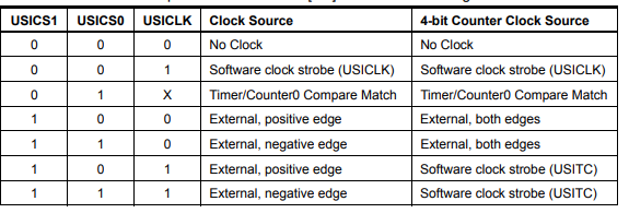 The synchronizing clock from SCL pin for this communication can be generated using USITC bit. The SCL pin state toggles from high to low and from low to high every time 1 is written to USITC bit.
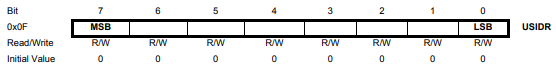
 USISR register bits with holds the status of the I2C communication. Each bits will reveal different status of the ongoing communication
 Steps to configure ATtiny85 to use I2C protocol and send data as Master:
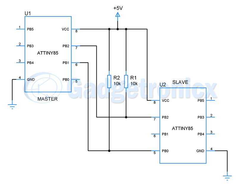


Hi, Thank you for this project.
I have a question. How can I do 10-bit addressing. I want 1000 Slave cards and 1 master card. I use ATtiny85 chip for slave cards. And I use ATSAM3X8e for master card.
Thanks for getting this code all in one place. Much of it looks accurate. However, I’ve noticed something.
while(USISIF==0); //Wait till address bit is received
That line is doing nothing. USISIF is a bit position number. According to the ATTIny85 datasheet it should equal 7. It is a constant and its value will never change. So that while loop will fall through immediately.
Further, although this is only slightly more than a knit-pick, the arrangement of a code block ({ … }) underneath it makes for a misleading code-read. The while condition’s code is actually a semi-colon no-op. The block is just a list of top-down code.
I cam across these tutorial whilst looking for examples for SPI interface on an ATtiny85, they are just what I am looking for.
What tool are you using for the software?
Hi, This article is very informative. Currently i’m looking for AtTiny 402 interfacing with RTC via I2C protocol. If you have AtTiny 402 I2C example code then it will helpful for me.
Hello I am following your tutorial on the I2C protocol.
The title of the section configuring the slave reads:
Steps to configure ATtiny85 to use I2C protocol and send data as Master:
This should be:
Steps to configure ATtiny85 to use I2C protocol and receive data as Slave:
regards Jos