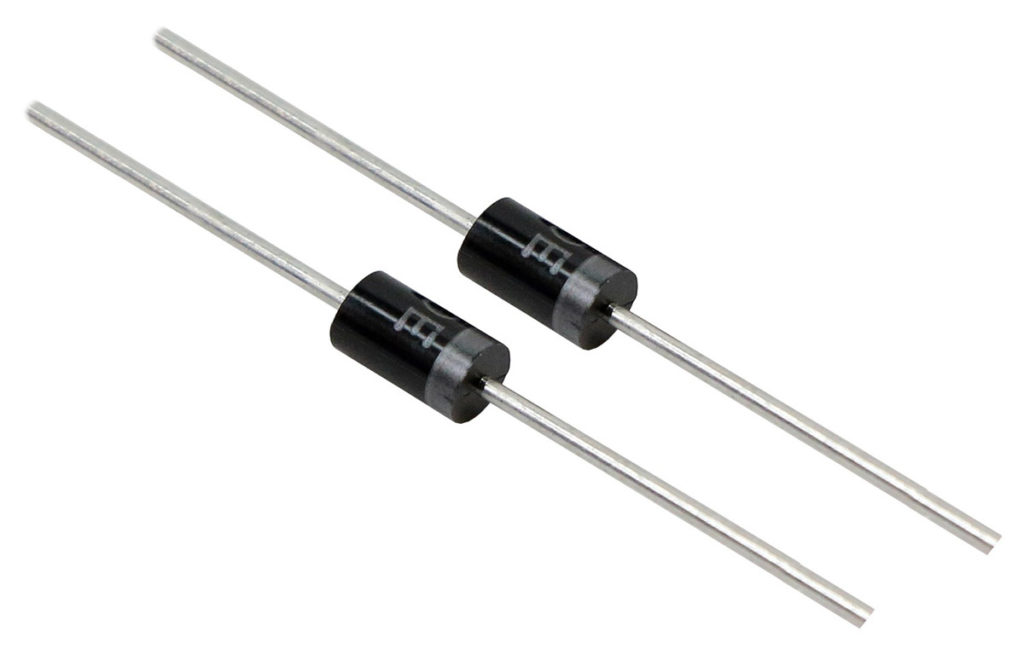
Diodes are often referred to one side valve and can be spotted in almost all electronic circuits. Diode is versatile component which has wide range of applications in areas such as power electronics, signal conditioning, power supplies, protection circuits and so on. In this electronic tutorial I will explain everything about Diode that you need to know.
This is Part 1 of Diode tutorial which answers your questions like “What is a diode?“, “How it is constructed?“ and “How it works?“ . Part 2 of this Diode tutorial will deal with its “Applications and how to use them in circuits“.
You can navigate to your preferred section of this tutorial using the below links.
Diode is a semiconductor device which has a peculiar property of allowing current when it flows from one direction and blocks them if the direction of current is reversed.
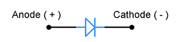
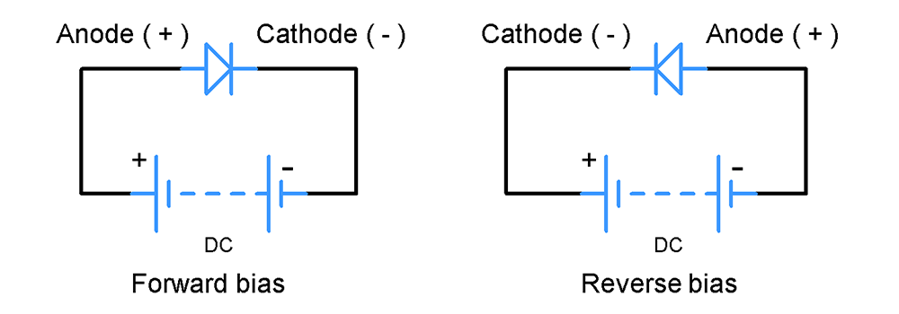
This is the symbol of a PN junction diode or commonly known as Diode where it has two terminals. Positive one which is known as Anode and Negative one which is known as Cathode. Here diode conducts current through it when its Anode terminal connects to positive terminal and Cathode to Negative terminal of a power supply. This condition is said to be forward bias of a diode and current flows through the diode freely.
When Anode of a diode connects to Negative terminal of a power supply and Cathode connects to positive terminal of a power supply. In this state current will not flow through the diode. This is said to be reverse bias of a diode and in this state diode exhibits infinite resistance blocking current flow through it. Although in practical life there will be very less current flows through the diode and it is defined as leakage current which is often deemed negligible.
PN junction diode is the most common type of diode that’s used till date in Electronic circuits. However there are other variants of diode in market which possess different characteristics than a PN junction diode. This tutorial focuses only on the working, characteristics and applications of a PN junction diode. I will cover other types of diode in another tutorial.
HOW DIODE WORKS:
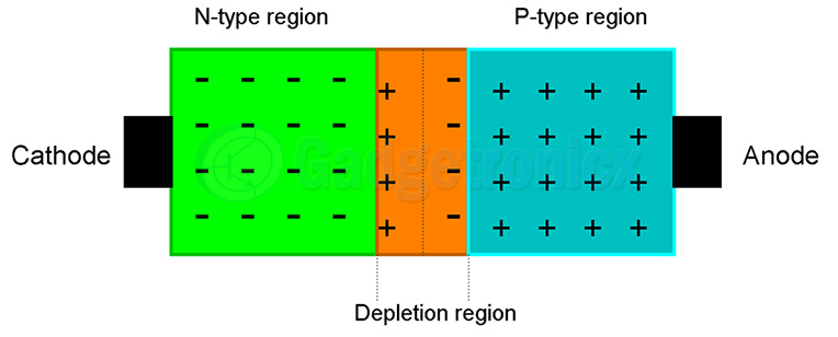
PN junction diode is made by combining a N-type semiconductor and P-type semiconductor together with a terminal attached to each of the P type and N type semi conductor material. The construction of diode forms the base for transistor and working principle remains same in both of these components. Anode terminal is connected to P- type material and Cathode terminal is attached to N-type material. For those who has little bit of exposure in semi conductors know that P-type semiconductor has holes as majority carriers and electrons as minority carriers. On the other hand N-type semiconductor generally means that it has electrons as majority carriers and holes as minority carriers.
For a PN junction diode P-type and N-type semiconductors are combined together. The point at which these two materials combine is referred as junction. The electrons from N type material and holes from P type material close to the junction will get attracted to each other because of opposite charges. Therefore holes from P-type material diffuses into N-type material and electrons from N-type region moves into P-type region forming a zone around the junction. The diffusion continues until the holes diffused into N-type region starts opposing further diffusion of holes from P-type region. And the same happens in P-type region where diffused electrons oppose further movement of electrons from N-type region.
This Electrons and Holes in the junction/ depletion region serves as a barrier for further ion movement. Also this indicates that free moving holes and electrons in that region is depleted. This leads to the name of depletion region. This depletion region as you see has positive and negative charges close to each other. This develops a potential of about 0.7v for silicon diodes across the depletion region. 0.3v in case of Germanium diodes.
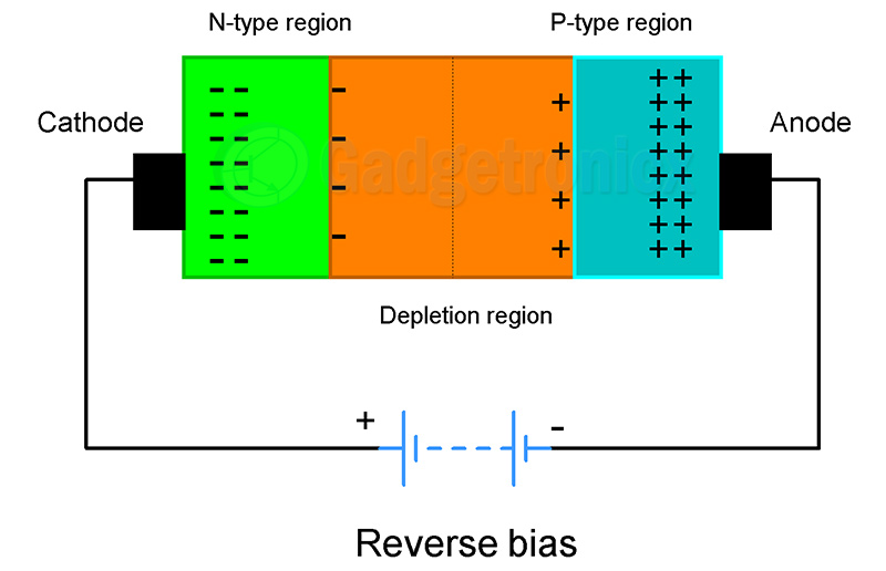
REVERSE BIAS:
So what makes this depletion region blocks current when reverse biased ? When a diode is reverse biased P-type material will be connected to Negative terminal and N-type region to positive terminal of power supply. As a result negative terminal attracts all the positive ions in P-type region close to it and Positive terminal attracts more negative ions in N-type region close to it. This results in further growth of existing depletion layer/ barrier in the junction thus blocking the flow of current completely. There comes a point when increase in reverse voltage will cause the barrier to break leading flow of current making irreversible damage to the diode. Thus by this means diode construction paves way for current flow only in forward biased condition.
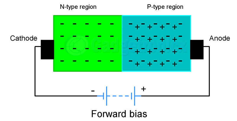
FORWARD BIAS:
On the other hand when a diode is forward biased positive terminal of a supply is connected to P-type material and Negative terminal is connected to N-type material. So when voltage is applied electrons usually moves from negative terminal to positive terminal. Same thing happens here, positive terminal attracts electrons from the depletion region and N-type material towards it. This happens when the applied bias voltage exceeds the barrier potential of 0.7v ( in case of silicon diode). As a result the depletion layer shrinks and vanishes allowing current to flow through the junction without any resistance.
Like explained above bias voltage must exceed barrier potential of depletion region ( 0.7v for Silicon diodes and 0.3v for Germanium diodes ) in order for current to pass through. This is referred as Forward voltage of diode. Sometimes it is also referred as Voltage drop of a diode since 9v forward bias across a diode will be 8.3v in it’s output dropping 0.7v.
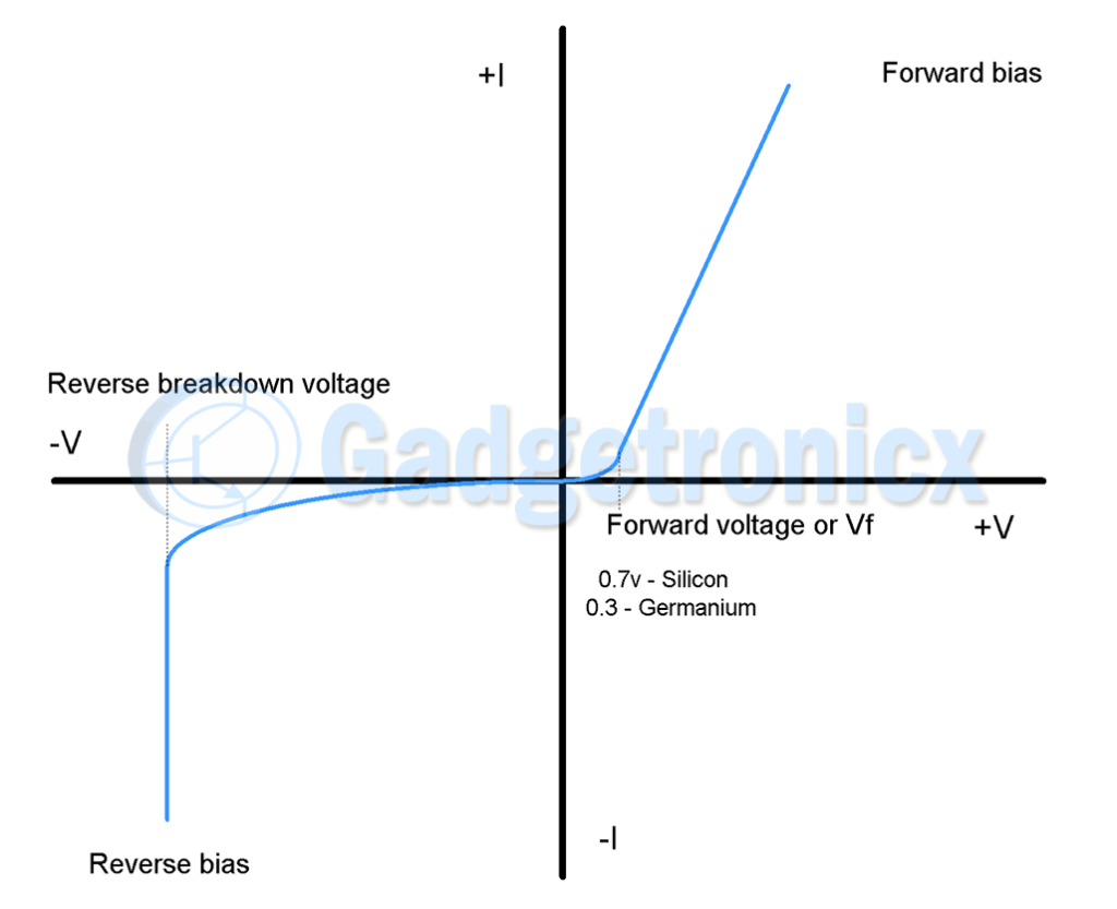
VI CHARACTERISTICS OF A DIODE:
It’s important to understand how voltage and current acts in a Diode. The below graph explains the relationship between voltage and current in a Diode. The right side of the graph shows the Forward bias condition ( Anode terminal is applied with more positive voltage than Cathode terminal) . Whereas in Reverse bias, this condition Cathode is more positive comparing to Anode.
When forward biased as you can observe at zero voltage, zero current will flow through the diode. As voltage continues to raise there is no real raise in the current flow. But once voltage applied reaches 0.7v mark ( for silicon diodes ) the current increases drastically reaching maximum value that diode will allow passing through it safely. This voltage is referred as forward voltage or VF of a diode. This forward voltage will be 0.3v for Germanium diodes. Also this forward voltage can vary from one diode of one type or material to another. This characteristic of diode will result in voltage drop of input voltage equivalent to this forward voltage value. Say a diode is forward biased with 5v applied across a Silicon diode the resultant voltage from cathode terminal of diode will be 4.3 ( 0.7v – forward voltage ).
When a diode is reverse biased no current flows through it until reverse voltage stays zero. When reverse voltage increases a very small current known as reverse leakage current starts flowing through the diode. This current is usually in the range of 0.000000001A or 1nA current has no notable effects in a circuit and therefore deemed insignificant. This is the reason Diode is claimed to be blocking the current totally in reverse bias condition.
After a certain point when you further increase the reverse voltage, current starts flowing rapidly through the diode. At this point diode will act like a short circuit allowing current to flow through it without any restriction. This voltage at which the current flows through diode without any restriction in reverse biased state is known as Reverse breakdown voltage. In most of the diodes exceeding reverse breakdown voltage will result in overheating and failure of a diode. Therefore you should always design in such a way the reverse bias voltage will not exceed reverse breakdown voltage.
SUMMARY OF DIODE:
Here is a short summary about Diode that will offer a quick refresh of what you have learnt above. Referring to below summary will be most effective if you would have gone through the above contents at least once.
Diode is a semi conductor device formed by joining P-type and N-type semi conductor together.
It conducts current only in forward direction that is when forward biased and blocks current when reverse biased
When forward biased applied voltage has to exceed forward voltage or voltage drop of a diode to force the current through it.
The forward voltage depends on the type of material diode made from ( 0.7v – Silicon diode, 0.3 – Germanium diode, 0.2v – Schottky diode )
In reverse biased state the current will be blocked until reverse bias voltage exceeds the reverse voltage of a particular diode.
If reverse bias voltage exceeds reverse voltage of a diode, it could permanently damage the diode.
Diodes are mostly used in applications such as Power circuits, Waveform modifiers, Protection circuits, Generators and so on.
This concludes the Part I of Diode tutorial. Hope this tutorial gave you a fair understanding of the science behind working of diode and how voltage and current acts in a diode. Part II of this diode tutorial deals with “Guide to use diodes and Applications of it“
This tutorial is part of our “Electronic components tutorial series” that we have been publishing in our website. Here is other tutorial that will be helpful to you.
Hope the above tutorials will help you to get better in Electronics. Kindly follow us through our Social media channels Facebook, Instagram, Pinterest, Twitter and subscribe to our Newsletter to get all updates regarding the circuits, projects and tutorials published in our website. Happy learning 🙂
David,
Am glad we could be of your help. Can you provide your feedback about our website please – https://www.gadgetronicx.com/feedback/ . It will help us to assess ourselves and do better
In the working diode, you have not given the symbols of donor and accepted properly. ‘Ions’ are to be circled. Otherwise confusion will arise wit ‘holes’


")
I love your way of teaching.it answers most of the difficult questions I have in my mind. It satisfies my curiosity
David,
Am glad we could be of your help. Can you provide your feedback about our website please – https://www.gadgetronicx.com/feedback/ . It will help us to assess ourselves and do better
In the working diode, you have not given the symbols of donor and accepted properly. ‘Ions’ are to be circled. Otherwise confusion will arise wit ‘holes’
Thanks for pointing it out. Will update the article