
Designing PCBs have become quite easier, thanks to the loads of tools available. For a beginner who is getting his hands on PCB designing, he may not be too much concerned about characteristics of trace used in PCB. However when you go up the ladder giving attention to PCB traces is of dire importance. In this article we have put together some important things that you should know about PCB traces and how to design the right traces for your PCB.
Also one important thing is to remember to check with your PCB manufacturer to see if they can manufacture the board with the given specifications. For example JLCPCB, a popular PCB manufacturer have their minimum trace width and spacing limit set to 3.5mil for multi layer PCBs. It is important to understand limitations like these and design your PCB that is within their limitations. In one of our previous article we have explained about basic PCB terminologies to be aware of for beginners, feel free to give that a read.
Trace width and thickness:
As you might know in a PCB, the copper lines which connect two points on the PCB, are called traces. A copper trace has a specific width, which we call trace width and has a specific height or thickness. The thickness is determined by PCB manufacturing company standards. You usually select Copper Weight with your quote, depending on your project requirements while ordering the PCB. It is measured in ounces and normally the copper thickness of a PCB is 1oz. Which means it’s the resulting thickness when 1 oz of copper is pressed flat and spread evenly over one square foot area.
Trace types:
In general there exist two types of tracks in a PCB. They are –
- Signal traces
- Power traces
Signal traces are those which carry data signals and power traces carries the current powering the circuit.
Power traces:
For power lines adequate trace width is necessary to ensure the desired amount of current can be safely transported without damaging the circuit board. The relationship between trace width and current carrying capacity in a PCB is pretty straightforward. A cross-sectional area of trace and temperature rise determine the current carrying capacity of a PCB. The cross-section of the trace is directly proportional to copper thickness and trace width.
Temperature rise:
This is a key factor which indicates the expected temperature rise is anticipated when the PCB is operating. This is usually affected by factors such as resistance, voltage drop, maximum current. There are other factors which influence this such as trace length, number of vias, pads and components etc. It is always a good practice to reduce high voltage drop which also reduces the power loss in your design to keep the temperature rise in check. Higher the temperature rise higher the PCB trace width will be.
Current carrying capacity:
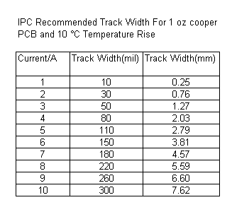
Higher current needs higher trace width. The IPC standard for the conductor thickness and width of the common 1 oz/square-feet PCB is as shown below. However, it is always advisable to use a bigger value due to the tolerance and variation of the PCB processes.
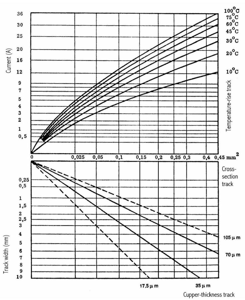
Credit: www.eurocircuits.com
Below image shows the recommended trace width against the current with 10c temperature rise.
Notice the track width increases with increase in current. Also if you need to calculate trace width for a specific current and other custom factors, there are several online tools available to calculate the width of a trace required to carry a given current while keeping the trace temperature below a specified limit. Actual results may vary depending on application and conditions. You can go to one of such websites to calculate as per your need.
Signal Trace:
Things get even more complicated with the signal traces or data lines, especially when you are working on high speed circuits. Things like signal integrity and trace impedance need to be considered in this case.
Signal integrity:
Putting this into simple words, Signal integrity is the tendency of an electronic signal to maintain its initial properties while travelling through a medium. A signal that is received with the same amplitude, phase, frequency, power and waveform as it had when leaving its source has high signal integrity. In reality this does not exist. Instead we use some designing tricks to keep the signal integrity at optimum level. Here is an article which explains about Signal integrity and design considerations that can help to achieve high signal integrity in your design.
Trace impedance:
This property comes in to play for high speed designs. For signals with high frequency, PCB traces don’t act like a simple connections. Every trace in PCB design has some series inductance, it can be often overlooked in low speed designs but in high speed designs this inductance will likely increase and affect the performance of the board. Adding to that every signal trace holds some capacitance value between the trace and its return path. These factors if left unchecked can deteriorate the performance of PCB since impedance will be different at different points in the PCB.
This calls for a method called as Controlled impedance in PCB designing where the designer should try to keep the impedance constant at every point in the circuit. This article explains the Trace impedance in detail and design considerations for designing controlled impedance PCB.
So these are the few things about trace width that you should consider while designing a PCB. I hope these tips will help you to make better accurate and complicated circuits boards. Though I have tried to cover major portions in this article I might have missed one or two things. If you have anything to add feel free to comment down below.


