Testing PCB or Printed Circuit Boards is an important process in PCB manufacturing. This process is as important as manufacturing itself. Testing process can save millions of dollars for the company and improve their product quality. In this article we are about to see common PCB testing methods. Besides explanation I have added related videos for better understanding of these testing.
Automated Optical Inspection ( AOI ) :
This is a common type of Non contact PCB board testing. Here Camera automatically scans the board for defects in the board. This AOI usually detects defects such as missing components, component placement, polarity, missing pad, short circuits and other defects that can be identified by visual checking. Usually the machine which carries out the AOI testing checks the board based on certain rules or by comparing it with actual board.
Automated X-ray Inspection ( AXI ) :
This method of inspection works pretty similar to AOI , however it uses X-ray rather than visible light to check the defects in the board. X-ray is capable of penetrating the board. This X-ray captured by a camera at the other side and this forms an image to check for defects. This X-ray testing method comes in handy to test Multi layer boards,IC connections, BGA chips where AOI inspection or Manual visual Inspection cannot reach.
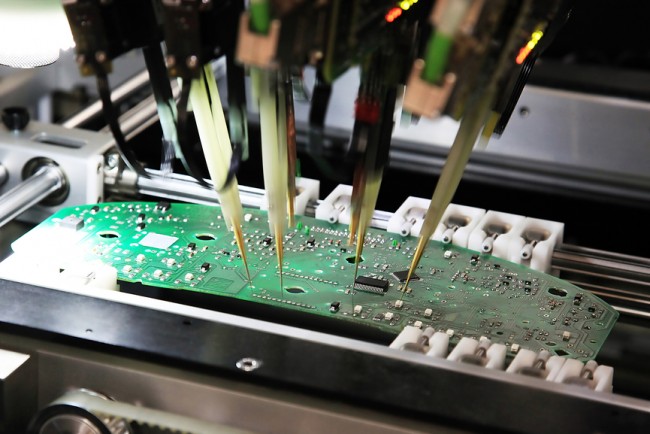
In-Circuit testing:
This is probably one of the oldest method of testing PCB’s but its still used by many manufacturers and it’s worth knowing about it. It’s performed by a bed of test nails usually Pogo pins will be used as test nails in the bed. During this testing these test nails will press against the board making electrical contact and then performs the test. In-Circuit testing is quite famous to detect Solder shorts, Solder joints, Resistance, Capacitance and common problems that occurs in PCB manufacturing and assembly.
Functionality testing:
This is one advanced form of testing where functionality of a PCB is tested. In previous tests we have seen so far it deals only with the fabrication and mechanical aspects of a board and detects any defect in it. However this functionality test simulates an Electrical environment for the PCB board under testing and check it’s functional response meets the acceptance criteria. This type of testing is usually carried out by connecting the board via Edge connectors or testing points. An automated machine will run the test on board and process the response received from the board. This type of testing requires special software or firmware for individual types of PCB’s to assess them against criteria such as Electrical response, Feedback, Frequency response and so on.
Functional testing gives an in depth understanding of boards functionality and how it will act in product environment. By this way manufacturers can assess its performance before delivering it to the customer.
JTAG Testing:
Joint Task Action Group commonly known as JTAG is an feature equipped in modern Microcontrollers and FPGA’s. So how does it test a PCB board is really interesting. So far the testing method we have seen uses an external device or equipment to perform testing on the PCB boards. But JTAG is a feature where a Microcontroller or FPGA can scan and test the PCB board for any defects. This can be done by means of JTAG programmers. These programmers are used to access I/O pins of controller and use it scan the PCB board for defects such as Shorts, improper soldering and so on. Also if the board consists of more than one JTAG supporting controllers then these components can be chained together to perform extended testing on the board.
So that’s all from PCB testing methods. These types of testing are still used by PCB manufacturers and Fabricators all over the world. This helps to improve their product quality. Hope I did my best to give a basic understanding about these tests and how it operate. Do check our website weekly for more informative articles and circuit. Also follow us via Social media channels and Subscribe to our Newsletter.