
Printed Circuit Boards or PCBs, make up an essential part of just about every electronic gadget you will ever see. Without PCB’s, electronic equipment would still be massive and take up entire rooms and there would be a huge room for error and faultiness. Thanks to PCB, the creation of electronic gadgets is now simple and cost-effective. While the PCB’s that are professionally manufactured make use of difficult-to-obtain and costly equipment but that doesn’t mean it is not possible to make PCB at home for your project prototypes.
Here’s everything you need to make your very own functional PCB in the comfort of your own home.
Materials Required to Make PCB at home:
- Laser Printer
- Clothing Iron
- Drill Machine
- PCB Board
- Glossy Paper
- Gloves
- Ferric Chloride
- Soldering Iron
- Sand Paper
- Black Permanent Marker
Most of these items are easily found at local electronic stores and office stationary shops.
Step 1:
First you need to have the full layout of the PCB you intended to make. Using software such as Autodesk Eagle or other famous software to build your PCB schematic is highly recommended but not mandatory. Some of the open-source PCB designing software is good as the paid ones, so do a bit of researching on their available software before committing to one. Once you chose your software design your PCB.
Step 2:
Once you done designing your PCB, check for any errors and correct them if any. Once the the circuit board is completely done, print a mirror image of the PCB layout into the glossy paper using a laser printer. It should look something like this
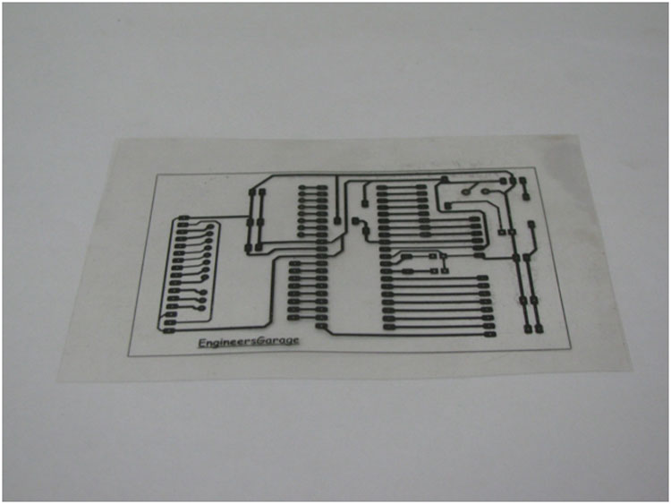
Image Courtesy: Engineersgarage
Step 3:
Now, take your copper clad PCB board you have bought from your local store and cut it to size based on the PCB schematic printed onto the piece of glossy paper. Remember to cut out the PCB a little bigger than your design.
Step 4:
Next, grab your sandpaper and rub down the copper-clad sideboard to remove the outer oxidized layer. This will make the glossy paper stick to the board easier for the next step in the process.
Step 5:
The next step is vital as you’ll be transferring the layout from the printed paper to the PCB itself. It’s vital that you printed a mirror image of the schematic because after transfer to the PCB, it will be back in the proper configuration. To accomplish this place the board near the printed schematic on the paper and then fold the paper over the board or place the copper side of the board over the top of the layout in glossy paper and then fold the paper around it. Works like a charm either way.
Step 6:
Take your clothing iron and get it hot. Now, run it slowly along the paper-wrapped PCB for 5-10 minutes to transfer the ink from the paper onto the board. After this, wait for the board to cool down, and then unwrap the folded paper. The paper can now be discarded. Any unfinished lines or places where the ink didn’t transfer properly need to be touched up using the black permanent marker. Now the copper board should look something like this.
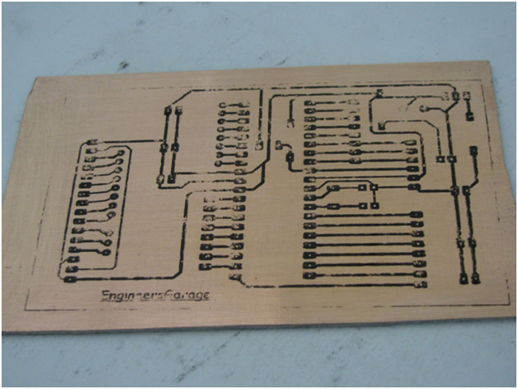
Image Courtesy: Engineersgarage
Step 7:
The only copper necessary is the copper stuck under the black lines left by the ink and marker, so this step involves removing the other copper from this side of the board. This is accomplished by adding approximately 2-4 teaspoons of ferric chloride solution to water. Colloquially, this solution is referred to as the etching solution. Leave the PCB within this solution for about 30 minutes to remove all of the copper except what’s under the black lines.
If there’s still unwanted copper after removing the PCB, then place it back into the solution for a bit more time. Afterward, wash the PCB with cold water, and you’ve completed the etching process.
Step 8:
Take your sandpaper again and use it to remove the black ink. Acetone placed on a cotton swab is another effective method of ink removal. If you’ve done everything correctly, you should now see the copper tracks running along the PCB.
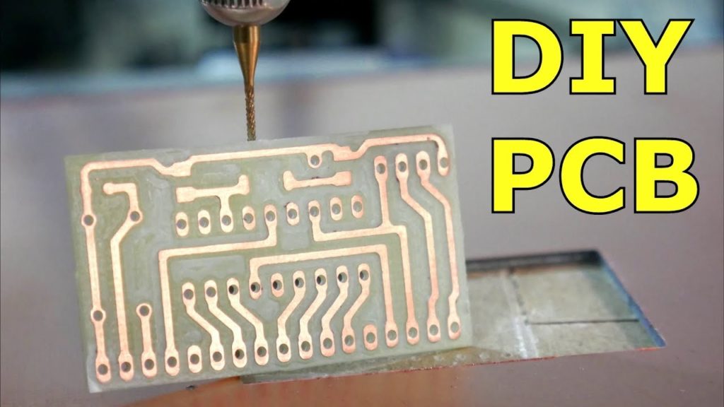
Step 9:
Drill the corresponding holes into the PCB according to the schematic using your drill. An Electric drill is recommended for gentle and precise drilling.
Your PCB is now ready and give a pat on your back you have successfully manufactured a PCB all by yourself.
Turning Your PCB Into a More Advanced Project:
The next step is to place all the components in the board and solder them in place before use. After you’ve created your own PCB, the next step of course is to integrate it into the intended gadget.
Manufacturers like NeodenUSA.com sell equipment perfect for low to medium volume batch for PCB production. This includes stencil printers and reflow ovens. Of course, you can still continue to do things by hand. But then, if you’re make PCB at home, chances are after a while you’re going to want a little bit of outside help.
With these machines, your homemade PCB’s can eventually turn into homemade electronic products with great quality.


