For hobbyist’s, engineers, and electronic enthusiasts, knowing the states of a logic circuit are important pieces of information. In addition, it is important to know what the frequency is of a pulse train. Is it in the audio, ultrasonic spectrum, (below 100 KHz), or the RF spectrum, (above 100 KHz). This article offers several low-cost methods that can be built to provide this information. There are three circuits for making a single state, ON or OFF, logic probe. The third circuit offers an add-on circuit which can determine if a logic pulse train is in the audio or RF spectrum. You can choose any of the circuit from the below that meets your requirement and cost and build one for yourselves.
LOGIC PROBE CIRCUIT:
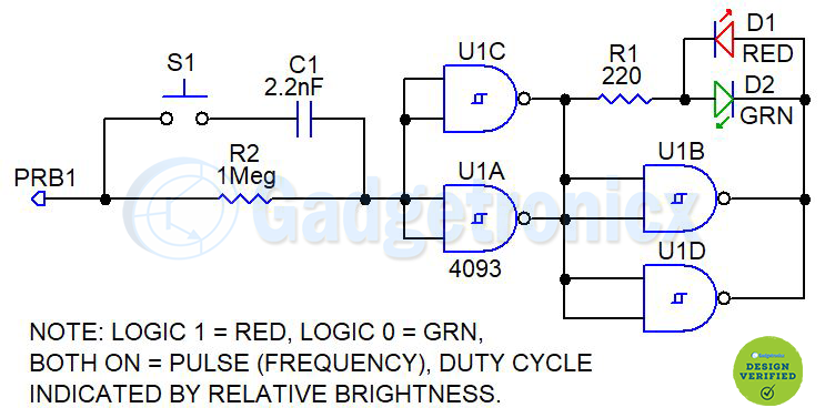
Figure 1
The first two such circuits are shown in Figure 1 and Figure 2. Each circuit is basically an input buffer comprised of a logic gate, and an inverter to drive the RED or GREEN LEDs to indicate the static state (level) of the logic circuit. Figure 1 shows a schmitt trigger NAND gate used as both the input buffer and the invertor. A common ground must be connected from the probe, to the circuit under test, to use the probe. The extra gates, U1C and U1D can be connected in parallel with U1A and U1B respectively to increase the current drive to the LED’s.
R1 limits the current through D1 and D2. Similarly R2 protects the input buffer from static and over-voltage. If needed, a N.O. push-button switch (S1) and small capacitor (C1) of 0022 uF (2.2 nF), can be connected in series, across R2 to improve high frequency sensitivity. Pressing S1 allows C1 to pass the high frequency signal around R2 to increase the sensitivity. As the note in figure 1 indicates, the duty cycle of the signal will be indicated by the relative brightness of the RED and GRN LEDs. The brighter LED will show the longer period of the duty cycle.
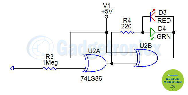
Figure 2
Figure 2 shows a TTL type of configuration using a quad, XOR gate connected as inverters by tying one of their inputs to +5 volts. Again, gates U2C and U2D can be paralleled with U2A and U2C to increase the LED drive. Also the switch and capacitor can be included like we did in previous circuit for increased high frequency sensitivity.
LOGIC PROBE CIRCUIT WITH FREQUENCY RANGE DETECTION:
Figure 3
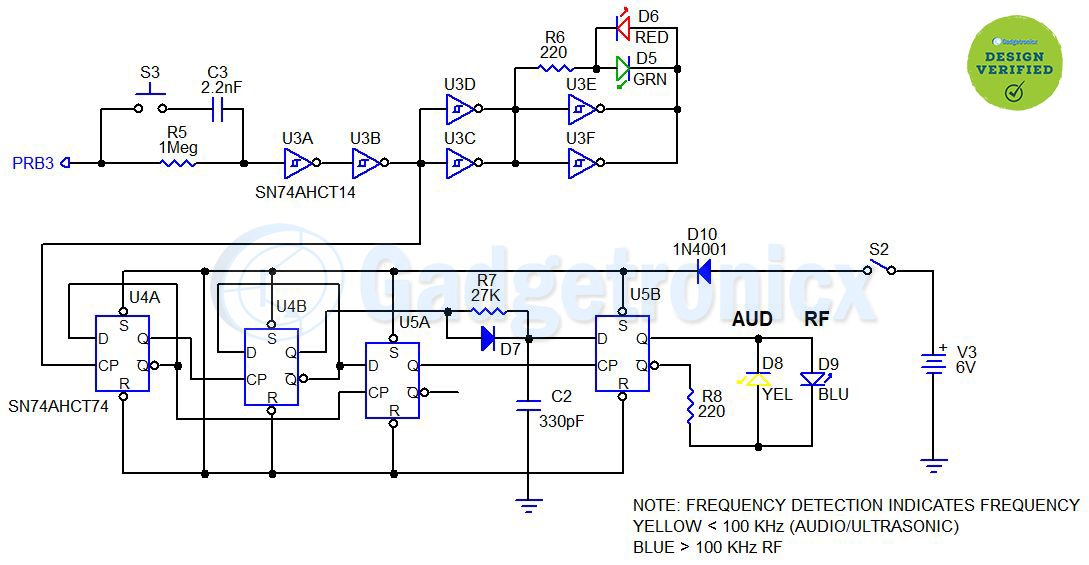
Figure 3 uses yet another type of gate and configuration for the static logic function. Invertor gates U3A and U3B form the input buffer while U3C, D, E, and F form the LED driver. The particular hex inverter gate, a SN74AHCT14, has schmitt trigger inputs which improve noise immunity on the input. They also provide up to 150 MHZ switching speed. The S3, C3 bypass circuit should be added for high frequency sensitivity.
Figure 3 includes additional circuitry which can measure the frequency of the input pulse train and therefore indicates whether it is above or below 100 KHz. This frequency is sort of a boundary between audio/ultrasonic and RF signals. The output from buffer U3B is used as the input to D flip-flop, U4A. As a result this cuts the frequency in half and provides a 50% duty cycle waveform regardless of the duty cycle of the input waveform. The Q output of U4A drives the clock input of U4B. The Q! (Q not, or Q bar) output of U4A drives the clock input of U5A. The Q not output of U4B serves as the data input of U5A. This results in a quadrature (90 degrees, out-of-phase), signal at the U4B Q output and U5A Q output. The Q output of U4B drives R7 and D7, that in turn charges C2, during the high output period.
During the low output period, C2 discharges through R7. Midway through the discharge period, the quadrature output of U5A goes high. This causes U5B to latch the data level of C2. If the discharge period is too long (low frequency), the voltage on C2 will be below the zero logical threshold. If the period is shorter (higher frequency), the voltage on C2 will be above the 1 logical threshold. Thus, U5A will latch a Q = 0, Q not =1, if the frequency is lower than 100 KHz, or Q = 1, Q not = 0, if the frequency is higher than 100 KHz. The value of R7 may need to be tweaked up or down depending on the family of logic flip-flops used.
A trim pot could be used for R7 to allow the frequency threshold to be adjusted. LED D8 (YEL) indicates when the frequency is below 100 KHz and LED D9 (BLU), indicates when the frequency is above 100 KHz.
LOGIC PROBE WITH FREQUENCY RANGE DETECTION PCB:
Figure 4
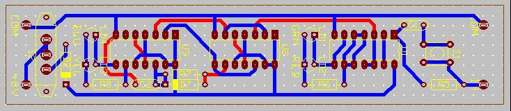
Figure 4 shows the PCB layout for the circuit in Figure 3. It includes a power diode (D2), ON/OFF switch (S2), pads for a +6 volt battery, (4 AAA, or 4 AA batteries), a ground probe pad, the momentary P.B. switch (S1) and high frequency bypass capacitor (C1).
For best high frequency results, use a SN74AHCT14 schmitt trigger hex inverter and SN74AHCT74 dual-D flip-flops. They are listed in the following BOM. Gerber files have been provided if a PCB is desired. PCBWay provides very good PCB boards at reasonable prices. You can download the Gerber files of this PCB below. You can order PCBs from www.jlcpcb.com , they have quick turn around time and builds PCB at low cost.
PCB design of Logic probe with Frequency range detection feature
Author:
Ron Hoffman
Platforms:
Windows 8
Category:
PCB designs
License:
Freeware
Date:
March 29, 2020
BILL OF MATERIALS:
ITEM
QTY
REF
DESCRIPTION
1
1
R5
1 Meg 1/4W carbon film resistor Yageo or equivalent.
2
2
R6,R8
220 ohm 1/4W carbon film resistor Yageo or equivalent.
3
1
R7
27K 1/4W carbon film resistor Yageo or equivalent. (May vary to calibrate for 100 KHz)
4
1
C1
330 pF film or mica capacitor.
5
1
C2
2.2 nF film capacitor Panasonic or equivalent.
6
1
LD1
Green LED
7
1
LD2
Red LED
8
1
LD3
Yellow LED
9
1
LD4
Blue LED
10
1
D2
1N4004, 1amp, 400 PIV diode.
11
1
D7
1N4148, silicon signal diode or equivalent.
12
1
S1
5mm N.O. push-button switch, EVQ-PAC09K, or equivalent.
13
1
S2
SPDT, SSW-91 miniature slide switch, ALL Electronics or equivalent.
14
1
U1
SN74AHCT14, schmitt trigger hex invertor, TI or equivalent.
15
2
U2,U3
SN74AHCT74, dual-D flip-flop, TI or equivalent.
16
1
PCB
PCBWay or HOFFMAN ELECTRONICS INC.
17
1
BPH
Battery pack holder, 4-AA or 4-AAA battery pack with leads.
18
4
BTRS
AA or AAA batteries.
This will be great addition to your workbench and helps you greatly when debugging digital circuits. Check out other Electronics Project in our website. If you have any queries/ feedback about this project, leave them in the comments section below.