Password based locking mechanism is a very popular method for safety of our prized possessions. Now with the rapid growth of technology, our locking systems are also modernized. New, better and more functioning Digital code lock have taken the place of old traditional locks, because it is small, secure and reliable than its mechanical counterpart. In this project we will see how to make this digital code locker without using MCU. In order to achieve this, we use logic gates, comparators, shift register to implement this.
How does the combination lock work?
This system has a preset master password and push buttons where user feeds the password. The input password length is restricted to five. Once five buttons are pressed, it is then compared with master password. If a match is found then relay gets activated unlocking the locker and green LED lights up. However when there is a mismatch, the locker indicates it by lighting up a Red LED.
Components required:
There are quite a lot of components used in this circuit. I have given a short description of each component’s function in the below list to better understand the circuit as you read further.
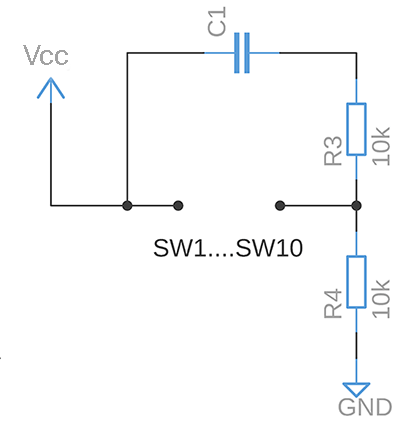
Push buttons – 10 (Input to the circuit)
74ALS520N – 2 ( 8- bit comparator to compare input with master password )
742G79DCU – 5 ( D type Flip Flop to temporarily store the input password )
74AS832N – 2 ( 5 Channel R gate to limit the input to five inputs )
74LS96N – 1 ( Triggers the comparison of input password with master password )
74ALS08N – 1 ( AND gate to combine the output from two comparators )
74LVC04 – 1 ( Complement the output to activate the alarm if password is a mismatch )
Relay
LED
Resistors
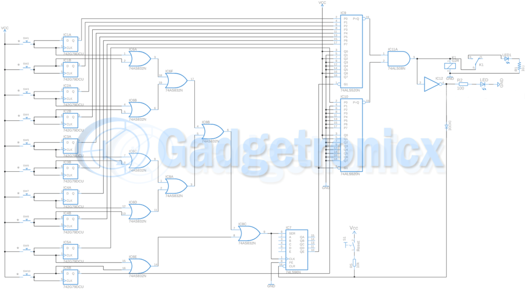
Digital code lock circuit diagram:
Working Principle :
The working of the above circuit is split into different blocks and explained individually.
Push buttons input:
We are using general purpose push buttons to feed Input to the circuit. When the push buttons are pressed it connects the input to Vcc. As a result high signal is fed to D-Flip flop to temporarily store it’s input value.
See the input terminal from push button marked as “*” ? This indicates the usage of debouncing mechanism with the push buttons. Push buttons are relatively slow compared to digital chips therefore chances are one press of push button will be interpreted as multiple inputs of same button. And this will lead to improper behavior of our locker circuit. To avoid this a combination of capacitor and resistor is added. When button is pressed Capacitor charges up but not instantaneously and it takes a while for Vcc to exhibit in the capacitor thus eliminating the possibility of exhibiting multiple button press to D- Flip Flop. Each buttons from SW1…..SW10 should use its own debounce mechanism setup. You can read more about this Debouncing mechanism and how it works in here.
D Flip-Flop:
As we can see one end of the Button is connected to Vcc and the other end is connected to Data and Clock pin of Flip-flop blocks. This is because, according to the truth table of D flip-flop, the output changes its state based on input to its Data pin but only when the clock pulse is active. So we need to pull both the pins high at the same time. So by pressing the button input of the Flip-flop and Clock pin goes High. Therefore we get High signal at the output. And it stays that way since Flip-Flop acts as a memory element here.
Comparator:
The output from Flip-flop then connects to input pins P0……P7 of the IC9 comparator and P0, P1 of IC10. The rest of the pins from P2 to P7 are connected to GND since we don’t need them. We need two comparator IC’s here, since we have ten input buttons and one comparator can only have 8 inputs for comparison. Here if you observe, other input states Q0….Q7 of IC9 and IC10 comparator are connected to either Vcc and GND. This will act as master password. You can use DIP switches for convenience.
You can notice Q0,Q2, Q6 of IC9 and Q0, Q1 of IC10 is connected to Vcc terminal here. This is being set as master password now. This means if user press SW1, SW2, SW7, SW9 and SW10 the pins of P0,P2, P6 of IC9 and P0, P1 of IC10 goes high and this will be put in comparison with Q0,Q2, Q6 of IC9 and Q0, Q1 of IC10. The comparison will result in output of IC9 and IC10 to go high indicating password match. If wrong buttons are pressed or buttons are pressed out of sequence output of IC9 and IC10 remains low.
OR Gate:
The button inputs are also connected to inputs of OR gates. And by the truth table we know that when either inputs of an OR gate goes high output also gets high. Each OR gate inputs are connected to two push buttons. So when any of them is pressed the output of that OR gate becomes high. Two outputs from the OR gate then connected to the input of another OR gate and so on leading to single OR gate. This OR gate is used along with shift register to limit the password input to five.
Shift Register:
We want to make it as a 5 digit code lock system. So we have to limit the password input to 5 buttons and compare the input password with master password using comparator. To limit the key inputs we will use a 5 bit shift register. We will connect the output from OR gate to input of this shift register. With each button pressed, binary counter on shift register will increase from QA to QE. The QE pin of shift register is connected to G1 pin of both comparators. Therefore upon five button press by user, QE goes high and it pulls G1 pin on both comparators high which commands the comparator to compare input with master password.
Comparison:
Once shift register activates the comparator, it compares the input logic on its P0….P7 pins with Q0….Q7 pins. If user pressed the SW1, SW2, SW7, SW9 and SW10 buttons in the right sequence, match occurs. This activates the output of comparators which goes to a AND gate. If user pressed incorrect buttons or buttons out of sequence comparator output will remain low and nothing happens.
Output stage:
When both the comparator’s output is high, output of AND gate goes high. The high output from AND gate activates the relay unlocking the locker permitting user to use it and green LED acts as an indicator. There is a reset button which is connected to CLR pin of shift register which should be manually activated by user to reset the locker back to it’s original state after usage. If the entered input is incorrect output of AND gate remains low and it will be inverted by NOT gate which will power up the red LED connected to it. The LED will be at this state until the user input right code and unlocks it.
Hope this circuit was interesting, educating and challenging to you. Also do check out other interesting Electronics projects in our website. If you have any queries, feedback about this project, do post them in the comments section below, we will address them. Do try this circuit and let us know about your results. Happy Making 🙂


Can we change the master password in this circuit? if no then how to implement the logic?
when press input 6 green light turned ON. by just pressing one button…