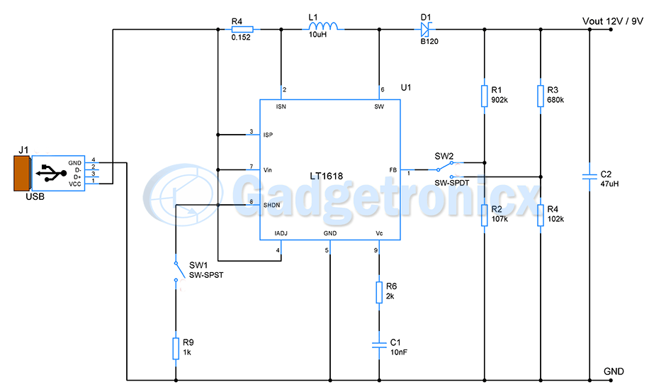
Voltage boost converters are used where we need to increase the incoming voltage from a given voltage source. USB power source has become very popular these days. The 5V output from USB power supply sources is very much readily available. With that in mind here is a circuit that boosts USB input voltage of 5V to 12V and 9V. This circuit uses a dedicated DC DC converter chip LT1618 from Linear technology and other discrete components to boost the incoming voltage.
Working of USB to 12V Voltage boost converter circuit:
The working of this circuit starts from USB power source. The Vcc and Gnd pins of USB connector connects and powers this circuit. The 8th pin – Shutdown pin of this Chip need to be pulled above 1V to turn this chip ON and in turn boost the incoming voltage. If Shut down pin voltage goes below 0.3V, LT1618 will cease working and therefore input voltage will not see any boost. The 4th pin IAdj provides a way to limit the output current to any specified limit. Applying voltage to this pin will modify the output current from LT1618. This adjustment is not necessary and therefore this pin is connected to high logic level.
The Vc or 9th pin of this electronic device is for compensation input for internal error amplifier. Compensation is not necessary for this circuit therefore a RC circuit with 2k and 10nF connects to this pin as advised in datasheet.
12V and 9V output voltage:
The most important aspect of this circuit is the output voltage. The output voltage from LT1618 IC is set by voltage fed into FB or 1st pin. This voltage input is set by using resistor pairs – R2 & R3 and R4 & R5. The output voltage from this boost converter is given by the formula
For the given values of resistors R1 & R2 and R3 & R4 the output voltage can be calculated as follows. Using this electronic circuit we are intended to boost the 5V input to 12V and 9V. Switching the SPDT switch SW2 to connect R1 and R2 resistor pair will yield 12V in the output. Whereas moving SW2 to connect resistor R3 and R4 pair will give 9V output.
Fixing the value of R2 as 107k in the above formula for 12V output will give Resistor R1 value as
R1 = 107k ( 12V / 1.263 – 1)
= 107k ( 8.502 )
= 909.7k
R1 = 902k ( nearest value )
Similarly for 9V using the resistor R3 and R4 we fix R4 value as 102k
R3 = 102k ( 9V / 1.263 – 1 )
= 102k (6.182)
= 630k
R3 = 680k ( nearest value )
Fixing the resistors R1, R2, R3 and R4 to above values will allow user to switch between 12V and 9V in output.
Inductor selection:
Datasheet advices us to use a ferrite core inductors to attain best efficiency. Also make sure to choose an inductor that can handle the maximum current delivered to the load. We have chosen to use 10uH inductor in this design. A Schottky diode B120 prevents the reverse current and also it provides low voltage drop from input voltage.
Hope this circuit was useful to you. Browse through tons of circuits categorized based on their functionality in our Electronic circuit library. If you have any queries or suggestions about this circuit do post them in the below comment box.


 Converter")


