
Meeting power demands in modern day electronics is quite a challenge and there are times where we will not be able to supply sufficient voltage for our circuits. In that case we need to go for DC to DC boost converter circuits like these to step up the incoming voltage to a certain usable level. These kinds of step up converter circuits will be useful in Solar powered projects, Lighting systems, Battery powered projects and so.
MT3608:
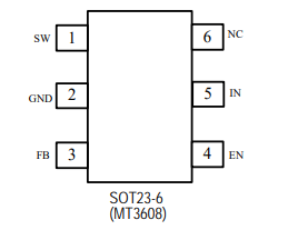
In order to understand the above circuit we need to understand this chip. MT3608 is a 6 pin DC to DC step up converter used to boost the incoming supplied voltage. Also this chip switches the load at about 1.2Mhz and only uses very few minimal external components to operate. Also it is equipped with under-voltage lockout circuit, current limiting and thermal overload protection just in case output tries to draw more current than its limit. This chip takes input voltage from 2 to 24V and Output voltage up to 28v and capable of delivering maximum current of about 4A. Checkout the Datasheet of MT3608 here for info about this chip.
WORKING OF 5V TO 12V BOOST CONVERTER CIRCUIT:
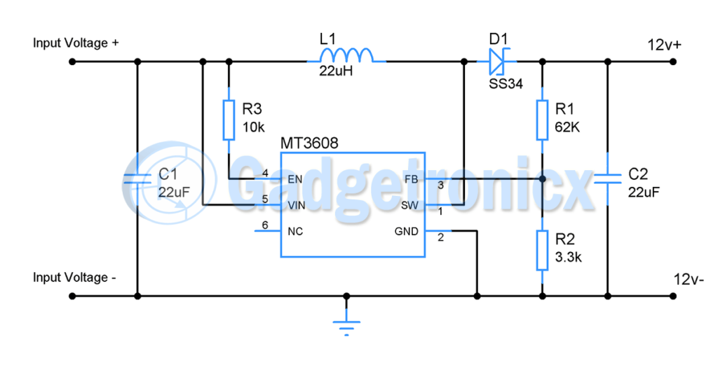
In MT3608 Chip, internally there is a power MOSFET that have its Drain pin connected to the inductor via SW pin and Source pin of Inductor is connected to ground. A typical MOSFET switch configuration. As soon as we power up the circuit the internal oscillator of MT3608 start to turn the MOSFET ON and OFF at a frequency of 1.2MHZ. When the MOSFET is in its ON state, the current coming through the Inductor passes through MOSFET to ground. Therefore when current passes through an Inductor, a magnetic field generates in it.
After a certain point internal MOSFET will be turned OFF. This point is decided by the voltage at the feedback pin provided by the voltage divider R2 and R1. The output voltage is governed by the formula
Vout = Vref x ( 1 + R1 / R2 )
where Vref is 0.6v.
After the MOSFET is turned off, the magnetic field of the Inductor turns in to voltage spike and it goes through the Schottky diode. Hence this voltage spike will be exhibited as output in the circuit. As there is a capacitor in the output, it charges in every cycle of oscillation and keeps the voltage constant. In this voltage booster circuit components are used to boost 5v to 12v. Above all for MT3608 to start working, the EN pin should be tied to high. If you want to turn on and off the output with an external circuit you can use this pin. This circuit is capable of delivering 2A current to the Load.
ADJUSTABLE OUTPUT VOLTAGE:
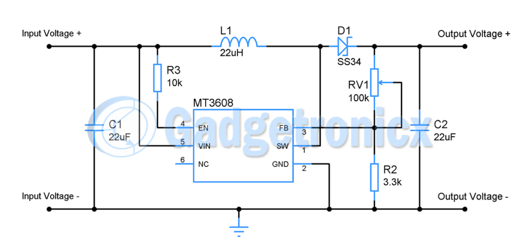
This circuit is similar to the above except output voltage in the circuit can be adjusted. As I already mentioned that output voltage is set by means of Voltage fed into the FB pin of MT3608. Here I have replaced the resistor R1 with Potentiometer PR1. As the resistance of POT changes the voltage in to the FB pin changes which in turn will change the output voltage accordingly.
Hope this Boost converter circuit will come in handy for your next projects. Feel free to post your comments, Feedbacks and questions regarding these circuits below. Bookmark our website and check it out weekly. New Projects / Circuits will be published on weekly basis.


Hello,
I am mostly a SW/FW engineer, not a HW guy (I know just enough to be dangerous!)…
I am trying to design a tiny PCB to repair some equipement (hence the tiny PCB, it HAS to fit in the existing housing), and I need to put a 5V to 12V booster to power a 2W stepper motor (3.5V*0.6A) through a A4988 stepper driver (Althrough, typically, the draw is only around 1.5W).
I have shared my project on easyEda at: https://easyeda.com/editor#project_id=9220fa26c27845ae8d1bbd93b3a543d9
Anyhow, here are the questions:
1) This design has a 22µF “output” capacitor. But I already have a 100µF capacitor as an “entry” to the A4988 stepper. PCB space is VERY limited for me. Can I just use the 100µF and drop the 22?
2) You are using a 22µH inductor, which is at the high end of what the datasheet says. I started my design by copy/paste of an existing easyEda project which was with a 4.7µH… what is the difference between the 2 choices? what would you recomend I use for my design? Would you have a part number to suggest?
3) Simillary to my question in 1), the 5V rail has 0.1µ, 4.7µ and 22µF capacitor, can I do the economy of at least one of these (once again, PCB space reducing)?
As I said, not an electronic engineer, hence my beginer questions… As a general rule, it seems that each IC is asking for input/decoupeling capacitor on 5V/VCC, is it ok to not put all these caps and reduce component load?
for info, my design is:
USB->ATTiny->A4988–>Stepper engine
|->5V->12V—-|
Thanks,
Cyriller
I am trying to boost the voltage to 12V using a lithium polymer battery.
What is the maximum output current? At least 6W of power is required.
This chip should be able to do that. You are looking at 0.5A output. But its worth noting the efficiency curve in the datasheet. As efficiency drops as the output current draw goes high.
What will be the R1,R2 when the Vout is 5v and vin is 3.7v?
It’s simple to calculate. The formula is Vout = Vref x ( 1 + R1 / R2 ) where Vref is 0.6v.
Fix any resistor R1 or R2 and calculate other values. Suggest you to fix R1 as say 10k and calculate the R2 using the above formula.
What will the R1,R2,Vin when I need 5.2v as vout
I am in a situation where Vout requires 12V.
The input voltage is fixed at 3.3V.
Through this post and datasheet, the formula of Vout = Vref x (1 + R1 / R2) was confirmed.
When the input voltage is 3.3V rather than 5V, is it okay to use the 5-12V example circuit of this post as it is?
If you take a look at MT3608 datasheet the input voltage has been specified as 2 to 24v. So 3.3v should work just fine.
Got the internal schematic got a feed issue keeps triping and shorting the curcit system as it could be a gate issue like on a RF 4 pin chip pnp type for app but blow the 4 pin line gate out swaped it for a nother all working good.
How did you calculate the Vref? I need to build a circuit to get 24V output.
The formula and Vref value is given in MT3608 datasheet.
Hi Frank, great Blog. I’m looking at building a PCB with 5 of these circuits on side by side with then the V+ & V- out connected together for higher amp. Would I need another Schottky diode at the end of each V+ out circuit before they connect to the other V+ out’s in the circuit?
I’m trying to develop a project for TEG’s where I’m gathering electrical energy from various sources.
Thanks John
John,
Would like to know more about what you are trying to achieve. What will be your input voltage and what is the output voltage you need to obtain?
Hi Frank, thanks for your response.
I’m working on a project where we must collect energy from various sources mainly from thermoelectric generators (TEG’s) attached to different heat sources. These will generate different voltages probably varying from 2v up to 5v. I firstly want to boost the voltage to a more usable 12v to 14v and equalise all the incoming voltages from the various sources then connect them in parallel. This can be then used to trickle charge a 12v battery.
Really my question is would I need to put another diode at of the end of each V+ booster circuit before the parallel connection or will the circuit work without this?
Thanks John
I see what you mean John, you explained this question very well. I suppose you can use a low forward voltage drop diode as you explained for added protection or perhaps you can add a single diode after the equalizing all the above voltages rather than using diodes at the output of each of these circuits.
Thanks Frank. This is what I thought, I just wanted a bit of expertise to confirm this. Thanks for your time.
Hi, You can’t build circuits like this cheaper than you can buy from Ebay.
I have been building electronics since 1972 and it was quite shocking to see the low prices in China including shipping to Norway.
That’s true. PCB manufacturers from China are capable of making PCB’s at extremely low cost and thus enabling us to get boards for shockingly cheap prices
can I use 2 of the circuit and wired in series to get a much higher voltage output say 50V? with the top circuit input v- tied to bottom circuit input v+ and 2 resistors to balance the input voltage.
No it won’t work that way.