Serial communication protocols provides the means to communicate for microcontrollers with external hardware, peripherals or other microcontrollers. USART, SPI, I2C are some of the popular serial communication protocols in embedded world. In order to facilitate serial communication in ATtiny85 microcontroller it is equipped with a Universal Serial Interface USI module. This USI module can operate in Two wire Synchronous data transfer ( I2C protocol ) and Three wire Synchronous data transfer ( SPI protocol ) modes. This tutorial covers how to operate ATtiny85 in both SPI master and slave mode.
SPI protocol or Three wire Synchronous data transfer mode:
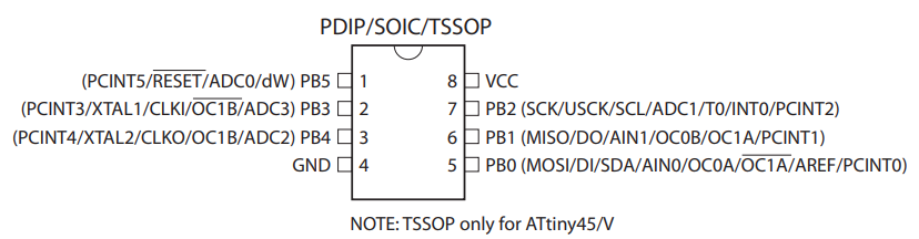
SPI is a form of serial communication that uses three pins to transfer data. In SPI communication the devices take the role of master and slave to establish communication. The master device is responsible for generating the clock pulse to synchronize the communication. Three mandatory pins of SPI communication in ATtiny85 are DO (PB1) , DI (PB0) and USCK (PB2). Additionally Slave Select ( SS ) pin can be configured in the code in case multiple slave devices are involved in the communication. Learn more about SPI communication in detail here.
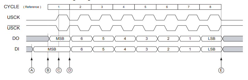
Timing diagram of SPI protocol in ATtiny85:
The above timing diagram briefs about SPI communication in ATtiny85. USCK is the clock cycle that synchronize the communication between devices. It can be external or internal ( generated by master device ). The data register associated with SPI communication is of 8 bit in length. DO shown above represents the data that goes out the sender device starting with MSB. DI shown above represents the data that comes in the receiver device starting with the MSB.
The point A and B at the above diagram represents that Data that need to be sent must be placed at the USIDR ( USI data register ) at least half a clock before USCK clock generation and the commencement of sampling. Also while receiving the data, MSB should be held in DI pin half a clock cycle before beginning of USCK sampling. This ensures sending of receiving of data bit in sync with the clock pulse. Each clock pulse will be sampled at rising and falling edges of the clock cycles. A 16 bit counter increments with each sampling ( rising and falling edges of clock pulse ).
The data bits 6, 5, 4,…. will be sent or received in sync with the trailing clock pulses. At the end of 8th clock pulse ( point E in above image ) all the 8 bits would have been sent or received and counter would have reached the maximum value. Upon reaching its maximum value Counter overflow flag raises indicating the data transfer is complete and now the next byte can be sent or received via data lines.
Slave select is the feature used in SPI when one master need to communicate with multiple slaves. For the purpose of slave select an individual pin must be assigned from the master device. If a master need to communicate with two slave devices two slave select pins must be assigned. When master device wish to send or receive data from slave-1 device, it will pull the slave select pin assigned to that slave-1 to low state. Now the slave-1 and master can communicate with each other.
In ATtiny85 there is no dedicated slave select pin. It need to be established by means of software meaning you to have use a IO pin and assign it as input if your device is a slave and when the input goes low, you need to activate the SPI communication. Whereas if your device is a master you have assign a IO pin as output and pull it to low to establish communication with a slave device.
USICR ( USI Control Register )
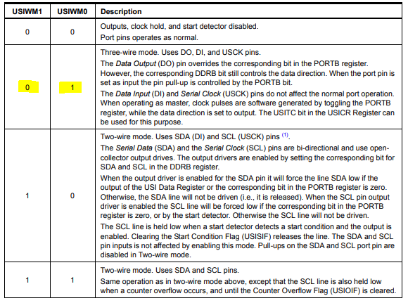
The bits USIWM1 and USIWM0 bits in the USICR register is used to set the USI module to operate using SPI protocol or I2C protocol. The below table shows the bit settings for choosing the SPI communication.
The bits USIWM1 and USIWM0 has to be set as 0 and 1 in order for our USI module to operate in SPI mode.
USICS0, USICS1 and USICLK bits are used to select the clock that will be used for SPI communication. The below table shows the various clock sources that can be used for our SPI communication and clock to power a 4 bit counter which is responsible for keeping the track of data sent or received ( explained below ).
Possible clock sources are Software generated using the USICLK bit, external clock to USCK or PB2 pin and Timer/ Counter0 compare match. In this tutorial we are going to use Software generate clock strobe ( USICLK ).
When USICLK bit is written as 1, single clock transition will be generated internally to power SPI communication. This enables USIDR register to send or receive single bit of data. Therefore bit has to be written high 16 times to send or receive a byte of data.
USITC is a bit that is responsible for generating clock pulse in case if we are using our microcontroller as master to generate clock pulse. Writing of this bit toggles the logic state in USCK pin from 0 to 1 or 1 to 0. This provides a way to generate clock pulse and synchronize data transfer with slave devices.
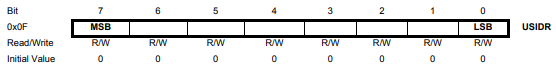
USIDR ( USI Data register ):
This the actual register which holds the data that need to be sent and the data that is received from other devices. User need to write 8 bit data in this register and then transmit the data by activating clock pulses to synchronize the transfer. Similarly when the ATtiny85 receives the data each bit received and placed in the USIDR register. When transfer of a byte is complete, data in USIDR register will be copied to USIBR register.
USIBR ( USI Buffer register ):
This is the similar to the USI data register. Contents of USIDR register will be copied to USI Buffer register when data transfer is complete. This provides user with time to read the data when the data transfer is time sensitive.
USISR ( USI status register ):
Status register is used to identify the status of USI peripheral. The bits USICNT0, USICNT1, USICNT2, USICNT3 are dedicated counter bits that keep count of the data transfer. It does that by incrementing by one every raising and falling edge of clock pulse. 4 bits are dedicated for this counter, therefore the count data will overflow after counting to 16, that is this counter will overflow after transfer of every byte.
In this register USIOIF bit is an overflow flag bit which will overflow when the above counter overflows after reaching 16 value. This flag will be read as one when a data byte transfer is completed.
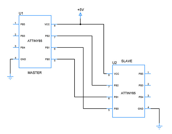
Circuit diagram – ATtiny85 MCUs as Master and Slave:
In this setup U1 acts like Master and U2 will be the slave. U1 generates clock pulse to synchronize this SPI protocol communication.
Steps to configure ATtiny85 and send data as master using SPI protocol:
Use the data direction register DDRB to set pins DO (PB0), DI (PB1) and USCK (PB2) as output, input and input.
Using the bits USIWM1 and USIWM0 bit in USICR register select the three wire mode aka SPI
Place the data byte that need to sent to slave in USIDR register
Clock the data transmission using the bits USICS1, USICS0 and USICLK. In this tutorial we are going to use Software strobe as clock so the these three bits will be written as 001.
Write the USITC bit high to toggle the USICLK pin which will serve as clock source to the slave.
Repeat the steps 4 and 5 until the USIOIF flag is raised to complete one byte data transfer
Write the next byte to USIDR register
Repeat the steps 4 and 5.
Sample Code for ATtiny85 as SPI master device:
#include<avr/io.h>
String tosend="Test";

void spi_setup()
{
  DDRB=(1<<PB1)|(1<<PB2);     //Setting direction of PB1 and PB2 as output
  USICR=(1<<USIWM0);          //Choosing SPI aka three wire mode
}

int main()
{
  short int i=0;
  spi_setup();
  for(i=0;i<=3;i++)
  {
   USIDR=tosend[i];          //Writing data bytes in Data register
   while(USIOIF==0)         //Checking USI data counter overflow flag to detect the end of transmission every byte
   {
    USICR|=(1<<USICLK)|(1<<USITC);  //Enabling clock for transmission and generating clock for slave device
   }
   USISR|=(1<<USIOIF);             //Clearing counter overflow flag
  }
}
ATtiny85 as SPI slave:
To configure SPI as slave device it need to be configured to take external clock pulse using USICS0, USICS1 and USCLK bits to take input from the master device. The input clock pulse from master device must be fed to USCK pin or PB2. The direction of this pin must be set to input using DDRB register.
Steps to configure ATtiny85 to receive data as SPI slave:
Use the data direction register DDRB to set pins DO (PB0), DI (PB1) and USCK (PB2) as output, input and input.
Using the bits USIWM1 and USIWM0 bit in USICR register select the three wire mode aka SPI
Choose the clock source as External positive edge and external both edges for 4 bit counter.
Wait until the USIOIF flag goes high, this indicates one byte has been received.
Copy the data from USIBR register for processing.
Repeat from step 4.
Sample Code for ATtiny85 as SPI slave device:
#include<avr/io.h>
String received[200];

void spi_setup()
{
  DDRB=(1<<PB1);     //Setting direction of PB1
  USICR=(1<<USIWM0);          //Choosing SPI aka three wire mode
}

int main()
{
  int i=0;
  spi_setup();
  while(1)
  {
   if((USISR&(1 << USIOIF))==1)         //Checking USI data counter overflow flag to detect the end of transmission every byte
   {
    received[i]=USIBR;  //Reading received byte from USIBR buffer register
    if(i<200)
     i=i+9;
    else
     i=0;
    USISR|=(1<<USIOIF);  //Clearing counter overflow flag
   }
  }
}
Try this out:
Set up two ATtiny85 with one being master and other being slave. Write code for both Master and Slave device with slave select functionality.
Master device should send a string “Welcome” and Slave responding back “Ok” upon successfully receiving the data.
Hi Frank
Further to my reply on Nov 10 2021 – I’m struggling and could do with some guidance. Just focusing on the SPI Master code, I can see PB1 toggling with data but it seems to happen in half the time PB2 is outputting a clock to the slave (in my case an AD9833 a waveform generator).
Referring to the ATTiny85 datasheet on USICR….
• Bits 3:2 – USICS[1:0]: Clock Source Select
Clearing the USICS[1:0] bits enables software strobe option. When using this option, writing a
one to the USICLK bit clocks both the USI Data Register and the counter.
And this is my confusion. In the “while((USISR & (1<<USIOIF)) == 0)" loop, each time "USICR|=(1<<USICLK)|(1<<USITC);" is executed, the data to send is moved left a bit (clocks … the USI Data Register) and the output clock state is toggled (clocks … the counter).
The counter overflows at 15 after 8 output clock pulses sent and seen on PB2.
But the data register got through its 8 bits of data (as seen on PB1) at a count of 7 because it changed at each toggle of the output clock.
This is also what I'm seeing on a scope – the data output seems to change on a clock transition (PB2) and there are then 4 clock pulses on PB2 after the LSB has been sent.
IE when 0b00000001 is output, this shows as a 'mark' coincident with the third clock pulse 'mark' – I'll try to illustrate below:
What have I done wrong? How can I eliminate the trailing 4 clock pulses?
Full disclosure – I changed your code to suit my needs but the crucial USI code should work the same. If you want to see my code I can send it but I guess this is not the forum.
when 0b00000001 is output, this shows as a ‘mark’ coincident with the third clock pulse ‘mark’ – I’ll try to illustrate below:
How about this…
PB2 (USCK) _ _ _ _ _ _ _ _
PB2 (USCK) ____ _ _ _ _ _ _ _ ____
PB1 (DO) _
PB1 (DO) ________ ______________
When 0b11000000 is output I see the following
PB2 (USCK) _ _ _ _ _ _ _ _
PB2 (USCK) ____ _ _ _ _ _ _ _ ____
Hi Frank
I think I fixed my issue – I now set USICS[1:0] as 0b10 – I do not understand why selecting the clock source as “External, positive edge” and 4-bit counter clock source to “Software clock strobe (USITC)” works as I’m using the internal clock as per your code example. Anyway, I now see data bits on DO (PB1) that line up with the clock pulse output on USCK (PB2).
Apologies for all the naff clock diagrams.
Are you able to explain why this makes the difference as it seems at odds with the datasheet?
Best regards
Peter
USIOIF is bit addressable so it is fine to use it as USIOIF==1. USIOIF bit will be one to indicate a byte of data has been received. So in the code we will check if it turns 1. Once it does the data is copied to received string. Writing 1 to the bit will clear this USIOIF bit.
Hi Frank
Thanks so much for this post – I’m a bit new to MCUs and have been bashing my head against a brick wall trying to get to grips with just talking to a wave form generator module. I started out with an ATTiny13A but these do not have USI support so I’d have needed to bit bang out each bit in the data – and they don’t have much flash anyway.
I started hunting round for an SPI.H that would work with my second MCU selection, the ATtiny85, and it seems that this is packaged with Arduino IDE for other MCUs.
What a relief to find out that the USI support on ATtiny85 can be put to good use. I read and re-read the ATtiny85 datasheet which only has assembler examples – I still struggle with the clocking options USICS[1:0],USICLK as [101] – (Software clock strobe (USITC)) – what does this mean in practice (it sounds a bit like the Software clock strobe (USICLK) [001] you use in your example?
Anyway – making some progress now – I have to agree with Tyler on his post – I tried your code addressing USIOF directly and nothing happened (as in scope attached to DO) – I had to reference the register USISR with this bit name – maybe you have some fancy IDE that supports direct bit addressing – I don’t.
In your slave code you reference this bit by looking at the register with the bit offset of USIOIF.
Thanks again – sometimes the hardest part of progress is to get the wheel rolling in the first place.
Bob, Thanks for pointing out the error. I have removed the int j and updated the code as well. Now i should roll back to zero once the string received is full.
Thank you so much for the help, im currently converting strings into byte arrays and sending them over to the slave device, i was wondering if you knew a better way to send and receive strings
Sure, the article is 80% completed. Originally it was planned to be published along with other articles but our team got busy. I will try to publish this by next week.
Hi Saph,
For slave device only direction of PB1 should be written as output. PB2 is only for master device which generates the clock. PB2 is meant for clock generation only in the master device.

 The above timing diagram briefs about SPI communication in ATtiny85. USCK is the clock cycle that synchronize the communication between devices. It can be external or internal ( generated by master device ). The data register associated with SPI communication is of 8 bit in length. DO shown above represents the data that goes out the sender device starting with MSB. DI shown above represents the data that comes in the receiver device starting with the MSB.
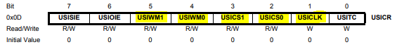
 The bits USIWM1 and USIWM0 has to be set as 0 and 1 in order for our USI module to operate in SPI mode.
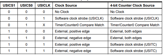
 This the actual register which holds the data that need to be sent and the data that is received from other devices. User need to write 8 bit data in this register and then transmit the data by activating clock pulses to synchronize the transfer. Similarly when the ATtiny85 receives the data each bit received and placed in the USIDR register. When transfer of a byte is complete, data in USIDR register will be copied to USIBR register.
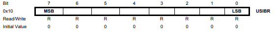 This is the similar to the USI data register. Contents of USIDR register will be copied to USI Buffer register when data transfer is complete. This provides user with time to read the data when the data transfer is time sensitive.
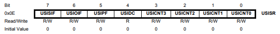
 In this setup U1 acts like Master and U2 will be the slave. U1 generates clock pulse to synchronize this SPI protocol communication.


if((USISR&(1 << USIOIF))==1)
how could this even work ? ==1 ?
USIOIF is the 6th bit, not the bit 0
did you even try this code ?
Hi,
In content 10 day is “ATtiny85 : I2C protocol – Master and Slave modes” but the link for this article is about SPI.
Is it available article about I2C with ATtiny 85?
Regards
Hi
Ok I found article under the link https://www.gadgetronicx.com/attiny85-i2c-protocol-tutorial/
Regards
hello
USIOIF is a macro equal to 6… in master, you check if 6 == 0 …
in slave : if((USISR&(1 << USIOIF))==1)
this dont check the bit USIOIF. 01000000 is never equal to 1.
just write if(USISR&(1 << USIOIF))
in slave, you dont enable any external clock input… it cant' works.
Hi
Gadgetronix i am getting eror while compiling your SPI slave device code in arduino IDE
Code:
#include
String received[200];
void spi_setup()
{
DDRB=(1<<PB1);
USICR=(1<<USIWM0);
}
int main()
{
int i=0;
spi_setup();
while(1)
{
if((USISR&(1 << USIOIF))==1)
{
received[i]=USIBR;
if(i<200)
i=i+9;
else
i=0;
USISR|=(1< Preferences.
Hi Frank
Further to my reply on Nov 10 2021 – I’m struggling and could do with some guidance. Just focusing on the SPI Master code, I can see PB1 toggling with data but it seems to happen in half the time PB2 is outputting a clock to the slave (in my case an AD9833 a waveform generator).
Referring to the ATTiny85 datasheet on USICR….
• Bits 3:2 – USICS[1:0]: Clock Source Select
Clearing the USICS[1:0] bits enables software strobe option. When using this option, writing a
one to the USICLK bit clocks both the USI Data Register and the counter.
And this is my confusion. In the “while((USISR & (1<<USIOIF)) == 0)" loop, each time "USICR|=(1<<USICLK)|(1<<USITC);" is executed, the data to send is moved left a bit (clocks … the USI Data Register) and the output clock state is toggled (clocks … the counter).
The counter overflows at 15 after 8 output clock pulses sent and seen on PB2.
But the data register got through its 8 bits of data (as seen on PB1) at a count of 7 because it changed at each toggle of the output clock.
This is also what I'm seeing on a scope – the data output seems to change on a clock transition (PB2) and there are then 4 clock pulses on PB2 after the LSB has been sent.
IE when 0b00000001 is output, this shows as a 'mark' coincident with the third clock pulse 'mark' – I'll try to illustrate below:
PB2 (USCK) ____-_-_-_-_-_-_-_-____
PB1 (DO) __________-____________
When 0b11000000 is output I see the following
PB2 (USCK) ____-_-_-_-_-_-_-_-____
PB1 (DO) ___–__________________
What have I done wrong? How can I eliminate the trailing 4 clock pulses?
Full disclosure – I changed your code to suit my needs but the crucial USI code should work the same. If you want to see my code I can send it but I guess this is not the forum.
Best regards
Peter
Dang – the font messed up the timing diagrams
when 0b00000001 is output, this shows as a ‘mark’ coincident with the third clock pulse ‘mark’ – I’ll try to illustrate below:
How about this…
PB2 (USCK) _ _ _ _ _ _ _ _
PB2 (USCK) ____ _ _ _ _ _ _ _ ____
PB1 (DO) _
PB1 (DO) ________ ______________
When 0b11000000 is output I see the following
PB2 (USCK) _ _ _ _ _ _ _ _
PB2 (USCK) ____ _ _ _ _ _ _ _ ____
PB1 (DO) __
PB1 (DO) ___ __________________
PB2 (USCK) ____-_-_-_-_-_-_-_-____
PB1 (DO) __________-____________
When 0b11000000 is output I see the following
PB2 (USCK) ____-_-_-_-_-_-_-_-____
PB1 (DO) ___–___________________
How about this…
_ _ _ _ _ _ _ _
PB2 (USCK) ____ _ _ _ _ _ _ _ ____
_
PB1 (DO) __________ ____________
When 0b11000000 is output I see the following
_ _ _ _ _ _ _ _
PB2 (USCK) ____ _ _ _ _ _ _ _ ____
__
PB1 (DO) ___ __________________
Hi Frank
I think I fixed my issue – I now set USICS[1:0] as 0b10 – I do not understand why selecting the clock source as “External, positive edge” and 4-bit counter clock source to “Software clock strobe (USITC)” works as I’m using the internal clock as per your code example. Anyway, I now see data bits on DO (PB1) that line up with the clock pulse output on USCK (PB2).
Apologies for all the naff clock diagrams.
Are you able to explain why this makes the difference as it seems at odds with the datasheet?
Best regards
Peter
SHouldn’t the USIOIF==0 check in the while loop be (USISR & (1 << USIOIF)) == 0 ? USIOIF is just a bit index.
USIOIF is bit addressable so it is fine to use it as USIOIF==1. USIOIF bit will be one to indicate a byte of data has been received. So in the code we will check if it turns 1. Once it does the data is copied to received string. Writing 1 to the bit will clear this USIOIF bit.
Hi Frank
Thanks so much for this post – I’m a bit new to MCUs and have been bashing my head against a brick wall trying to get to grips with just talking to a wave form generator module. I started out with an ATTiny13A but these do not have USI support so I’d have needed to bit bang out each bit in the data – and they don’t have much flash anyway.
I started hunting round for an SPI.H that would work with my second MCU selection, the ATtiny85, and it seems that this is packaged with Arduino IDE for other MCUs.
What a relief to find out that the USI support on ATtiny85 can be put to good use. I read and re-read the ATtiny85 datasheet which only has assembler examples – I still struggle with the clocking options USICS[1:0],USICLK as [101] – (Software clock strobe (USITC)) – what does this mean in practice (it sounds a bit like the Software clock strobe (USICLK) [001] you use in your example?
Anyway – making some progress now – I have to agree with Tyler on his post – I tried your code addressing USIOF directly and nothing happened (as in scope attached to DO) – I had to reference the register USISR with this bit name – maybe you have some fancy IDE that supports direct bit addressing – I don’t.
In your slave code you reference this bit by looking at the register with the bit offset of USIOIF.
Thanks again – sometimes the hardest part of progress is to get the wheel rolling in the first place.
Thanks for this.It seems there is a mistake in slave code.
“i” is implemented but never get back to 0. And “j” is declared but not used.
Bob, Thanks for pointing out the error. I have removed the int j and updated the code as well. Now i should roll back to zero once the string received is full.
Thank you so much for the help, im currently converting strings into byte arrays and sending them over to the slave device, i was wondering if you knew a better way to send and receive strings
ATtiny85 supports one byte per transmission, so the method you are using is the right one to do.
Could you also do one for I2C? I’ll gladly donate something.
Ernesto,
Sure, the article is 80% completed. Originally it was planned to be published along with other articles but our team got busy. I will try to publish this by next week.
Thanks! Looking forward to it
thank you for this explication, i want to make the slave responding , do I need to change the direction of PB1 and PB2 in the slave?
Hi Saph,
For slave device only direction of PB1 should be written as output. PB2 is only for master device which generates the clock. PB2 is meant for clock generation only in the master device.