It all started with an existing over 30 years old REX Datentechnik 9628 Extern Kernal 8 board (Date codes of the main parts: 1988). I got really intrigued to reverse engineer and learn about its function and the way a Kernal cartridge is different from a generic EPROM cartridge for the Commodore C64. The described reverse engineering method is mainly based on optical/photographic procedures. And I thought to write a guide on how to perform this process of Reverse engineering. A decent knowledge of the GIMP, Photoshop or any other image processing software, that offers layers is required.
What is Reverse Engineering:
It is the process of duplicating a product without the help of any documentation of drawing of any sorts. Here we are going to look at Reverse Engineering a PCB board where we attempt to recreate the design by means of visually inspecting them and conducting some tests on the board.
Required Tools
Digital Camera
Scanner
Image Processing software like GIMP or Photoshop (elements)
Soldering iron
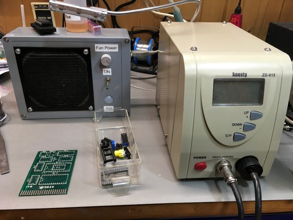
Solder sucker/De-soldering station (see Figure 3)
E-CAD program (like Eagle, KiCAD etc.)
Multimeter/LCR-Meter
Printer
Pencil
Good concentration
A sense for electronics and some experience
Step 1: Test the Function
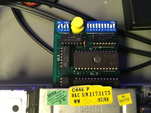
Figure 1: REX9628 in the expansion port of the C64
First it has to be proved, that the circuit is working. This is not always necessary, but quite helpful to know that all parts on the board are still working. You might need to measure some parts in order to identify them. Also, it is good to know a bit about the function and gain as much information as possible before the final schematics is drawn.
Step 2: Take a Good Picture
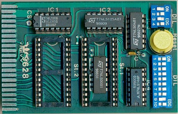
Figure 2: A scan of the assembled REX9628 board
One or more high resolution pictures is required to document the position and reference number of parts on the PCB. A scanner can do a great job, here. In case the parts on the PCB are not too high, that scanned picture looks very decent and sharp enough. All pictures should be checked to be sharp and all parts are visible before the next step.
Step 3: Catalog the Parts and Unsolder
Figure 3: Unsoldered REX9628
In this step, the parts have to be identified and their values have to be documented. In this case, it is fairly easy, because most parts already have reference numbers (like IC1, IC2 etc.) which are printed on the PCB and all values are printed on them clearly. The DIP-Switches are standard, the RESET switch, too. The capacitor value is most probably 100n and does not really matter.
In other designs you might have to define the reference numbers/designators and write them over or beside the part on that picture from Step 2, then document the values referencing to their designators. The GIMP is a software tool that helps with this job. Some parts have to be measured after unsoldering.
Identifying the part values or manufacturer part numbers is a critical step. In case a part cannot be identified or replaced with a suitable other part, it might make the reverse engineering impossible. The identification of connectors and small SMD parts can be very challenging. A catalog of SMD codes can be very helpful. Search for “SMD code book”.
The parts have to be kept well in a way, that they cannot be confused. Many little (anti-static) zip-lock bags and/or jars, paper labels and a pencil can be very helpful. The simplicity of the described project has allowed to drop the parts into a plastic box and keep the ICs on an anti-static foam mat.
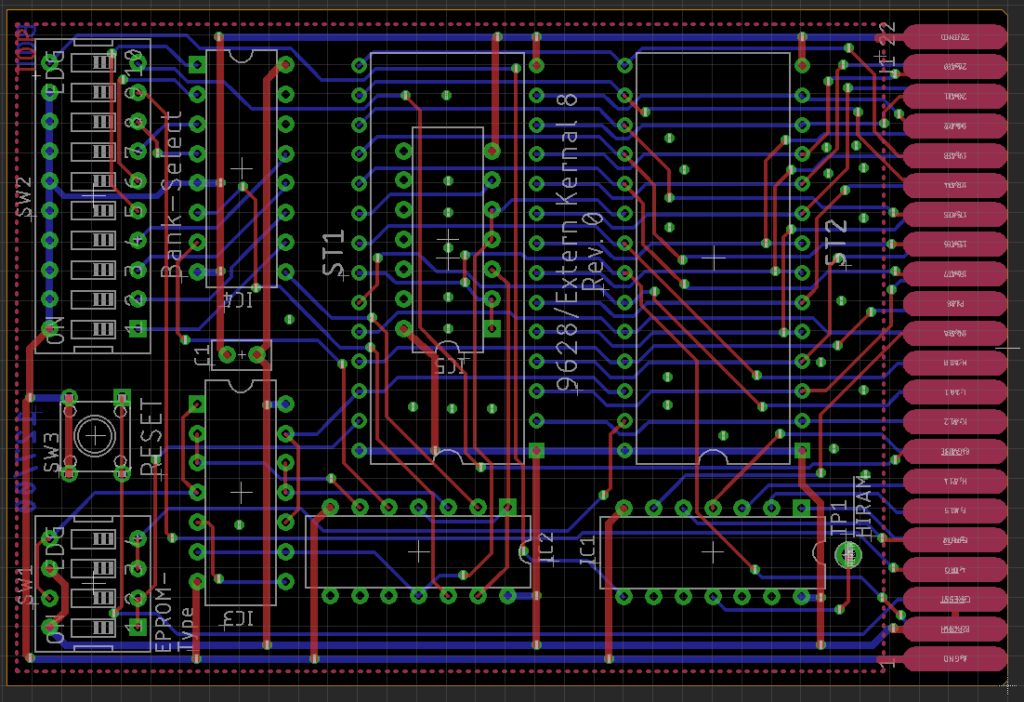
Step 4: Scanning the PCB and Image Processing
This reverse engineering method is based on image processing. First, both sides of the PCB are scanned in a decent resolution (e.g. 300dpi). Later the scans are assembled with an image processing software like the GIMP. The goal is to resemble a PCB CAD view of the board with both layers in different colors viewed from above the component side.
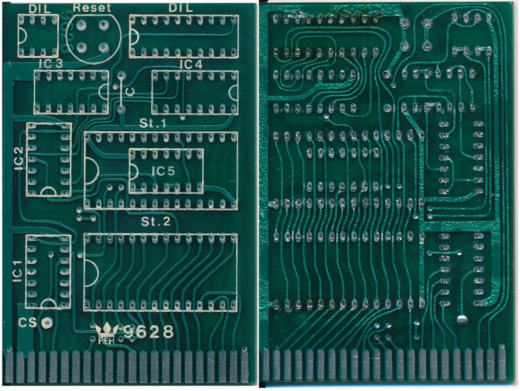
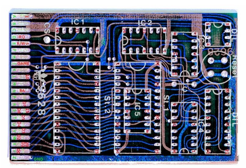
Figure 4: Both sides of the PCB
Figure 5: CAD view of a different PCB layout ( For reference )
Figure 6: Photographic overlay of the copper layers (bottom layer is blue, top layer is red)
These two layered scan was dyed to resemble a CAD view shown in Figure 5 for better understanding.
The process with the GIMP:
Create a new image, a bit bigger in size as the scans of the PCB to allow alignment
Set the background color of the image to black.
Insert the scan of the solder side right above the background layer
Mirror this scan
Replace the color of the non-copper areas with “transparent”. This might not work perfectly. It might even be required to erase some still visible non-copper areas in case they are disturbing.
Dye the remaining copper traces blue (or your preferred CAD tool color setting)
Insert the scan of the component side above the bottom layer
Replace the color of the non-copper areas with “transparent”
Set the opacity of the top layer to about 75%, so the bottom layer becomes visible
Align both layers
Add a “silk screen” layer, if required. The REX9628 already had such a position print
Add one or two layers with pin numbers to help counting pins later. The numbering of the edge connector on the solder side is a bit odd, so the numbering of those pads was required.
Add as many signal names as known
You need to store the file for later use and also a print to follow the copper traces with a pencil.
Step 5: Datasheet and CAD Library Work, Placement
Getting the required data sheets and creating the part libraries in the CAD program has to be done before starting to draw the first schematic. Since usually the parts that belong to the same functional group in the schematics are close together on the PCB, too, it is advised to place all components resembling their relative placements on the PCB. After the copper traces have been “transformed” into signals on the schematic, this schematic will usually be rearranged.
Step 6: Traces to Signals
Paper and a pen/pencil are the main tools of this step. The traces are followed with the pencil on the print obtained from Step 4. The pin numbers assigned before are now very helpful. The pencil marks the traces which are already followed. Concentrated work is required and multiple checking, since a mistake will cause a fail of the reverse engineering or at least lead to a time-consuming debugging. In doubt, the image processing software (GIMP) will provide a better view and finally, it is required to check connections with a beeper.
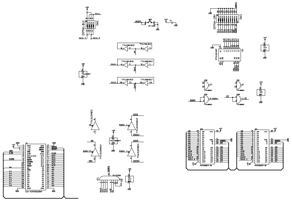
Making use of signal names/labels is more useful than drawing a signal cluster/ravel, that rather resembles the PCB view from before. The signals should be named reasonably, the naming might change later. This is the first step to gain understanding of the circuitry. The result of this step is shown in Figure 7: First pass of the schematics Figure 7.
Step 7: Trying to understand the circuitry and rearranging the schematic
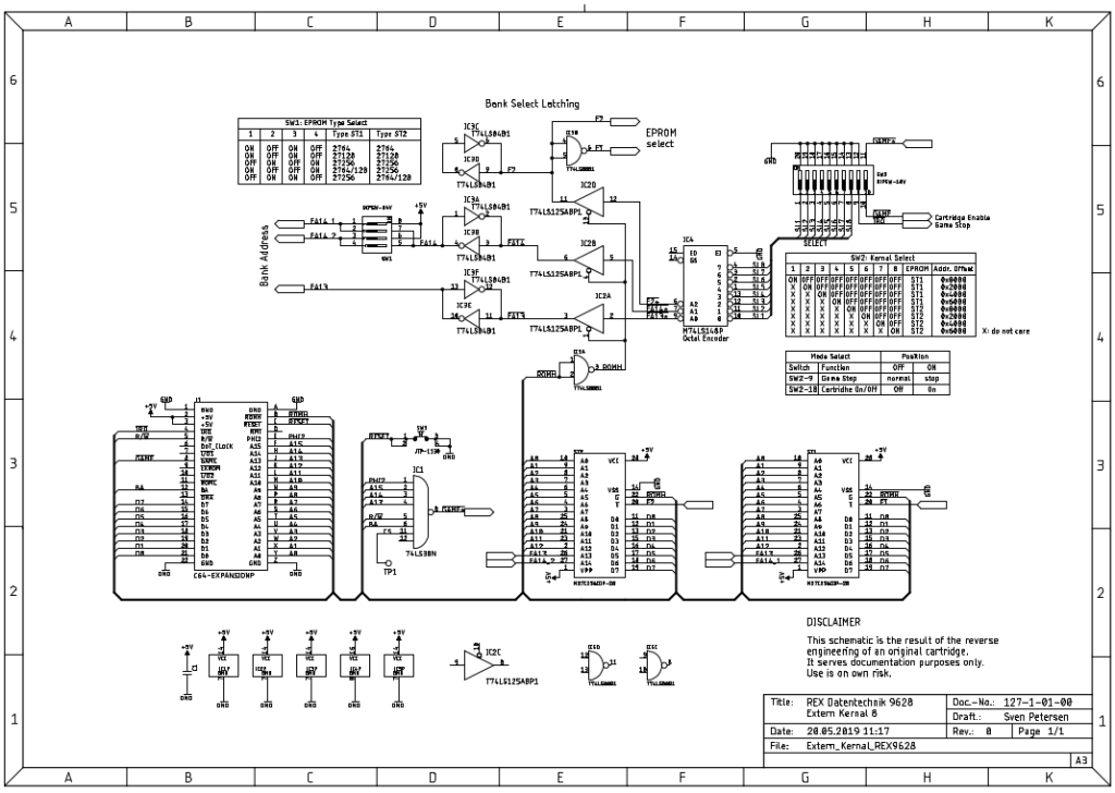
The next step requires electronic expertise. The circuit has to be reviewed and understood. Any oddities have to be carefully investigated on the physical PCB. In case of the REX9628, it was the IRQ being switched to ground with the DIP-switch that seemed to be strange. It turned out to be the “Game Stop” mechanism. After the functions of the components and circuitry was understood (the 74LS148 required a datasheet with a logic table), the schematic was rearranged rather reflecting the function than the placement on the PCB. Some Signal names were improved. See Figure 8.
Finally, the gained knowledge was documented. The board layout (refer to Figure 5) was lastly created.
Figure 7: First pass of the schematics (Result of Step 6)
Figure 8: Final schematic of the REX9628
Motivations for Reverse Engineering:
I have been working as a hardware developer for almost 25 years, mostly in engineering services and has taken part in a number of reverse engineering projects. Those were done out of different motivations.A copyright infringement must not be the intention behind this kind of work. In most cases, a new hardware development is easier to accomplish than copying a PCB and it is usually cheaper. In many cases, a reverse engineering is not possible or require methods that cannot be conducted by an average engineering service, such as grinding a multi-layer PCB to scan all copper layers or intrusive methods to regain the programming information of a code protected micro-controller. A scenario of “we cannot buy the processor anymore, but we want to keep the code” is usually a show-stopper, because an emulation of this processor (or other vital parts) is an expensive undertaking.
In most cases, customers depend on their development service, but did not request the full documentation and source files. Over the years, it gets more and more difficult to produce the board due to obsolescence of parts, the original developer is not available anymore and when it starts to be threatening for a company, the CEO starts looking for an alternative, having little information consisting mostly of oral traditions. Usually a PCB design is “a project” for the development service and “the project” for the customer. And those are very often not able to determine, if the “files” they have received (if the have received them) are most recent and complete. Usually, they are not.
Also, in aviation or railway applications, the vehicles have a much longer life cycle than the electronic components built into them and it is a challenging task to keep those vehicles running and to get hold of the obsolete parts. In depth information about the electronics are not available in some cases. The electronic modules usually have to undergo costly certification processed, so there is enough funds to pay for a reverse engineering to get something, that is not too different from the original to shorten the re-certification. In several cases, it is intended to produce some service manual, which requires a schematics.
To automatize the reverse engineering, a group of companies gathered, discussing the possibility of a CT scan (computed tomography) of a PCB, automatic optical inspection and measurement with a flying probe tester. Finally creating schematics, PCB production data and documentation. As of my knowledge, this project was not led to a success.
The component identification is a very difficult part of the reverse engineering process. Absolute maximum values can be assumed, but not measured. Tolerances cannot be measures as well. Some steps require more expertise than developing a circuit. And finally, a specification is required to really verify the result. A specification of a module/PCB in a complex system is a moving target throughout a development process. The initial specification defines requirements, the final module has properties and the corresponding modules might have to be adjusted to those in order to get a running system.