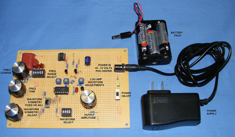
Function generators are quite expensive and due to that many engineers limit themselves by not getting one for their workbench. This hinders many testing and prototyping opportunities. Gladly there is a work around for this, a DIY Function generator that can produce Square, Sine and Triangle wave with adjustable frequency. This project is a improvised version of DIY function generator which was published in our website earlier. Unlike the previous version, this FG comes with logarithimic sine wave converter and improved efficiency.
CIRCUIT DIAGRAM:
Working of Function generator circuit:
Triangle and Square wave:
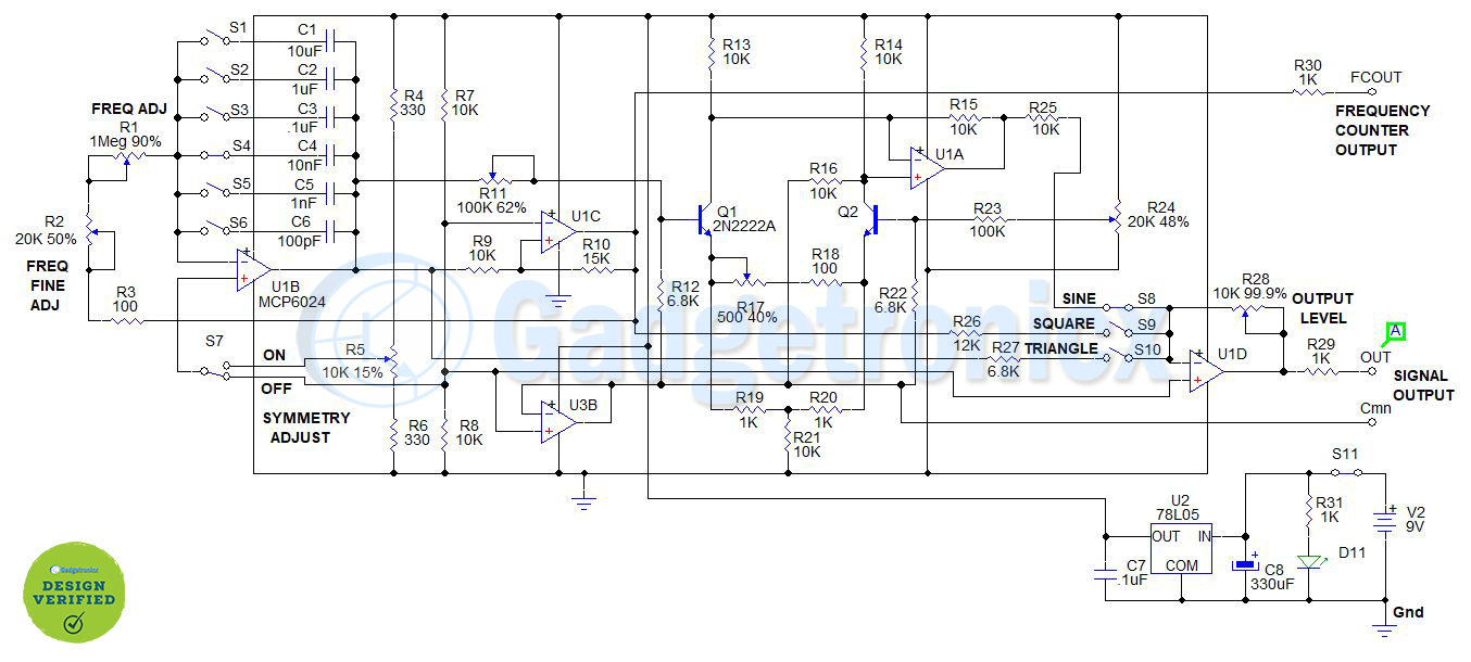
Refer to the schematic in Figure 1 for the following theory of operation. The heart of the function generator is the integrator, formed by U1B, R1, R2, R3, S1- 6, C1 – 6, and the comparator with hysteresis, formed by U1C, R6, R7, R9, and R10. They work together in the following way. U1C has its output low. When the input feeding U1Bin- is less than the reference voltage, the output of U1B ramps up. The output of U1B is connected through R9 to input U1Cin+. When the voltage at U1Cin+ is greater than the reference voltage at U1Cin-, (half of the supply voltage), the output of U1C goes high. This raises the voltage at U1Cin+ causing U1C to switch states. Since the output of U1C is higher than the reference voltage at U1Bin+, the output of U1B begins to ramp down. When the output of U1B through R9 pulls the input U1Cin+ lower than U1Cin- reference, U1C output switches low. This causes U1B to again begin ramping up until the output of U1B causes the input U1Cin+ to go higher than U1Cin-, and the process repeats in an oscillating manner. The output of U1B is a triangle wave. The output of U1C is a square wave.
Sine wave:
To produce a pseudo-sine wave, the output of U1B is connected by R11 to the base of Q1. Q1 and Q2 are connected with coupled emitters to form a logarithmic amplifier. R11 controls the amplitude of the signal into the log amplifier. R17 adjusts the emitter loads to adjust the waveform symmetry of the sine wave. R24 adjusts the offset symmetry for the logarithmic amplifier. Each control must be adjusted several times to achieve the best sine wave waveform with the least Total Harmonic Distortion (THD). Careful adjustment of R11, R17 and R24 should yield a THD reading of about 0.5%. The output of the logarithmic amplifier is fed into a ground referenced (Common, Cmn) node to buffer the sine wave and shift the signal referenced to Common.
The outputs of U1A, U1B and U1C are connected through R25, R27, and R26, respectively, to the input U1Din-. R28, a 10K potentiometer, provides the appropriate feedback to control the output level of U1D, from zero to Vmax. R29 protects the output of U1D and couples the signal to the output jack. Selector switches S8 – 10 are used to select the desired output type of waveform, sine, square, or triangle. Switches, S1 – 6, are used to select different values of capacitance, (C1 = 10uF, down to C6 = 100pF, in decade steps), to change the frequency range of the function generator. R1 provides the coarse frequency adjustment. R2 provides the fine frequency adjustment. Switch, S7, connects integrator input U1Bin+ to either +V/2 at the junction of R7 and R8, or the wiper of R5. R5 can be adjusted to nearly +5V or ground, to create a saw tooth wave at the output of the integrator U1B, or a pulsed square-wave signal. R30 is used to protect the output of U1C while providing an output signal to an external frequency counter or oscilloscope trigger. U2 is a 78L05 regulator that reduces the battery or power supply voltage (9 to 12 volts) to 5 volts to supply the function generator circuitry. U3B provides the common reference that is approximately one-half of the 5 volt regulator voltage (+V/2 = 2.5 volts).
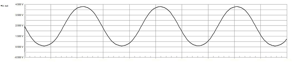
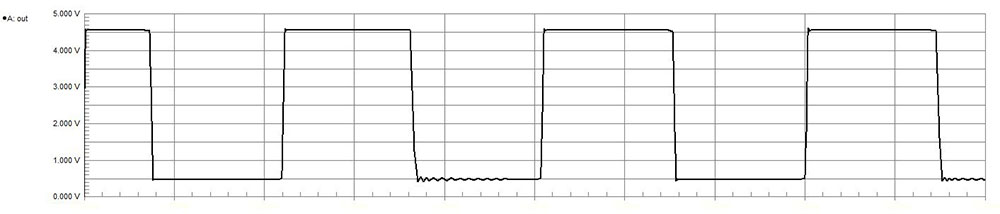
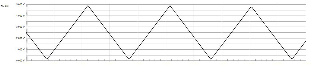
The quad op-amp chosen is a Microchip technology MCP6024. It is an RRIO (Rail-to-Rail, Input, Output) type that operates at 5V – 5.6V. It has a slew rate of 10V/uS which allows higher frequency operation without sacrificing waveform integrity. Figures 2, 3, and 4, show sine, square and triangle output waveforms respectively.
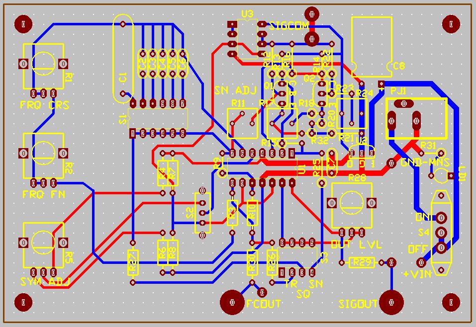
Gerber files of Improved Function generator PCB design
Author:
Ron Hoffman
Platforms:
Windows 8
Category:
PCB design
License:
Shareware
Date:
April 10, 2020
WAVEFORMS:
Figure 2 : Sine wave
Fig 3: Square wave
Fig 4: Triangle wave
BILL OF MATERIALS ( BOM ):
ITEM
QTY
REF
DESCRIPTION
1
1
C1
10 uF metallized film capacitor
2
2
C2,C7
1uF metallized film capacitor
3
1
C3
0.1uF metallized film capacitor
4
1
C4
0.01uF metallized film capacitor
5
1
C5
1nF metallized film capacitor
6
1
C6
100pF metallized film capacitor
7
1
C8
330uF, 16v, Alum.Electrolyric capacitor
8
1
D11
Green LED
9
1
R1
1M potentiometer
10
1
R2
20k potentiometer
11
2
R3,R18
100 ohm,1/4 W carbon film resistor
12
2
R4,R6
330 ohm, 1/4W carbon film resistor
13
2
R5,R28
10k potentiometer
14
9
R7, R8, R9, R13, R14, R15, R16, R21, R25
10k, 1/4 W carbon film resistor
15
1
R10
15k, 1/4 W carbon film resistor
16
1
R11
100k trim potentiometer
17
3
R12, R22 R27
8.8k, 1/4 W carbon film resistor
18
1
R17
500 ohm, trim potentiometer
19
5
R19, R20, R29, R30, R31
1k, 1/4 W carbon film resistor
20
1
R23
100k, 1/4W carbon film resistor
21
1
R24
20k trim potentiometer
22
1
R26
12k, 1/4 W carbon film resistor
23
1
S1-S6
6-position DIP switch
24
2
S7, S11
SPDT mini slide switch
25
1
S8-S10
3-position DIP switch
26
2
Q1,Q2
2N2222A, NPN transistor
27
1
U1A-D
MCP6024, Quad op-amp microchip technology
28
1
U2
78L05, 5v regulator
29
1
U3A-B
MCP6022 dual op-amp microchip technology
30
1
J1
2.1×5.5mm coaxial power jack
31
1
V2
6-“AA” or “AAA” battery holder and batteries (optional)
32
1
P1
2.1×5.5mm coaxial power plug
33
1
V2
9-12 V, 1A or 2A power supply, center positive
This project will be improve your workbench by great deal. And you don’t have to restrict your projects anymore. There are more useful and functional electronics projects in our website, take a look. Post your questions, feedback and improvement ideas in the below comments section below, we will address them.
Just wondering, what is the voltage output of this signal generator? I’m looking for a unit with at least 5 volts or more at the output to fire a large scr for the purpose of voltage chopping in a power supply.
Hi Ron,
first of all thank you very much for sharing your knowledge.
Can we have a call for a couple of improvements I find useful?
Or some email exchange…
Thank you again, kind regards,
Alex
Hello Ron,
first of all thank you for sharing your project.
I’m thinking about building a function generator like this for my diy escapades, yor circuit is really close to what I have in mind, I’m quite sure it can be adapted without too much effort.
Here are my ideas:
– supply the board using an old recylcled transformer (how many VA? Not much, I suppose…), using both half waves and the centre tap to generate the dual supply, for a bigger amplitude (if needed)
– using a couple of dual opamps and one single opamp instead of a quad opamp and a dual opam wasting one opamp
– socketing the opamps, so that it’s possible to try several types to increase the maximum frequency (ie TL072, but can be tricky for latch-up, or Opa627, for a very high slew-rate, or anything else suitable)
– using a single pole n-throws to select frequency range and type of output, thus becoming fool-proof, at least for the output
– putting the finished object in a fancy box, containing the power supply too
What do you think about it?
I have a couple of recycled transformers of little power (3 to 10VA), about 6,3V, 12V, 12-24V.
What do you think about it? Can the circuit be adapted?
Hi Pratik, First, what do you mean by simulation? Did you build the actual circuit or are just simulating it in a SPICE software emulator? If you have built the hardware, set the balance control R17, and offset control R24, to the center position. Control R11 adjusts the gain into the logarithmic amplifier which shapes the triangle waveform into a pseudo-sine waveform. If R11 is too small, the waveform will appear to be clipped. Adjust R11 until you see the best shape. The SINE WAVE text section describes how must adjust the three pots to obtain the best looking sie waveform. Hope this helps you.
Thank you sir for replying and i am doing simulation in online simulator and i have used opamp 741 instead pf mcp ic’s and i will see through the pot’s values and check for sine wave thank you
Hi Pratik, You have just told me what is wrong. A 741 op-amp has several characteristics that cause the simulation error. First is the high input current they require compared to the super low current needed by the MCP6024 and MCP6022 which are CMOS input op-amps. Second, the MCP606x op-amps are rail-to-rail input and output, or RRIO. The 741 cannot pull up to within only 1.5 volts of the upper rail and to about .5 volts above the lower rail. Third, the slew rate of a 741 is about 1V/uS compared with 10V/uS for the MCP602x family of op-amps. This severely limits the frequency bandwidth and waveform shapes due to the diminished high frequencies. That being said, the biggest problems are the input bias currents and the limited input and output range. If you simulate or build the circuit using the correct amplifiers, it will work correctly.
Hi Pratik, First, what do you mean by simulation? Did you build the actual circuit or are just simulating it in a SPICE software emulator? If you have built the hardware, set the balance control R17, and offset control R24, to the center position. Control R11 adjusts the gain into the logarithmic amplifier which shapes the triangle waveform into a pseudo-sine waveform. If R11 is too small, the waveform will appear to be clipped. Adjust R11 until you see the best shape. The SINE WAVE text section describes how must adjust the three pots to obtain the best looking waveform. Hope this helps you.
Hi Peter, My bad. The schematic value of 20K is correct I must have accidentally double hit the 0. Sorry about that. It is a 20 K trim pot used to adjust the bias offset. Let me know how it works for you when you have it done. Thanks. Ron
Hi Ron, just finished this project and it works great 🙂
I found a few things to mention that can be helpful for other hobbyists.
1. The switches in the schematic do not match with the PCB. So S1 on the PCB is S1…S6 in the diagram. S2 is S7 in the diagram. S3 = S8…S10 in the diagram. S4 = S11 in the diagram.
2. The LED symbol on the PCB is reversed.
3. In the picking list line 17 8,8k resistor is mentioned. In the diagram 6,8k is mentioned. I used 6,8k.
4. Resistor R19 is on the PCB marked as R32
I hope this helps others.
Thanks and greetings from The Netherlands
Hi Peter, thanks for the feedback. Since the dip switch unit (S1) the layout software counts it as one where it is really S1 – S6, so S2 is really S7. The four dip switch unit used for the waveform selection becomes S3, and the Power, (ON/OFF) switch becomes S4. Sorry for the confusion. The square pad and flatted outline symbol indicates the + lead for the LED. That is the convention I always go by. The 8.8K is a typo and should be 6.8K as is shown on the schematic. Thanks again for your feedback. I’m glad it works well for you. Regards, Ron.
Hi Ron, can you advise on how to connect the signal output/common to another circuit (an small amplifier circuit for example) with it’s own power supply / ground.
RON HOFFMAN
Hi Peter, The signal generator output ground reference is SIGCOM pad on the PCB. It is the Vdd/2 output from U2B. Since the function generator is powered by either the isolated, switching power supply, or a battery pack, the function generator will “float” relative to the SIGCOM reference ground.


Just wondering, what is the voltage output of this signal generator? I’m looking for a unit with at least 5 volts or more at the output to fire a large scr for the purpose of voltage chopping in a power supply.
Hi Ron,
first of all thank you very much for sharing your knowledge.
Can we have a call for a couple of improvements I find useful?
Or some email exchange…
Thank you again, kind regards,
Alex
Hello Ron,
first of all thank you for sharing your project.
I’m thinking about building a function generator like this for my diy escapades, yor circuit is really close to what I have in mind, I’m quite sure it can be adapted without too much effort.
Here are my ideas:
– supply the board using an old recylcled transformer (how many VA? Not much, I suppose…), using both half waves and the centre tap to generate the dual supply, for a bigger amplitude (if needed)
– using a couple of dual opamps and one single opamp instead of a quad opamp and a dual opam wasting one opamp
– socketing the opamps, so that it’s possible to try several types to increase the maximum frequency (ie TL072, but can be tricky for latch-up, or Opa627, for a very high slew-rate, or anything else suitable)
– using a single pole n-throws to select frequency range and type of output, thus becoming fool-proof, at least for the output
– putting the finished object in a fancy box, containing the power supply too
What do you think about it?
I have a couple of recycled transformers of little power (3 to 10VA), about 6,3V, 12V, 12-24V.
What do you think about it? Can the circuit be adapted?
Kind regards,
Alex
hello, very nice ckt but while simulation I am not getting Sine wave proper, could you please help me with that.It will be very thankful if you do so.
Hi Pratik, First, what do you mean by simulation? Did you build the actual circuit or are just simulating it in a SPICE software emulator? If you have built the hardware, set the balance control R17, and offset control R24, to the center position. Control R11 adjusts the gain into the logarithmic amplifier which shapes the triangle waveform into a pseudo-sine waveform. If R11 is too small, the waveform will appear to be clipped. Adjust R11 until you see the best shape. The SINE WAVE text section describes how must adjust the three pots to obtain the best looking sie waveform. Hope this helps you.
Thank you sir for replying and i am doing simulation in online simulator and i have used opamp 741 instead pf mcp ic’s and i will see through the pot’s values and check for sine wave thank you
Hi Pratik, You have just told me what is wrong. A 741 op-amp has several characteristics that cause the simulation error. First is the high input current they require compared to the super low current needed by the MCP6024 and MCP6022 which are CMOS input op-amps. Second, the MCP606x op-amps are rail-to-rail input and output, or RRIO. The 741 cannot pull up to within only 1.5 volts of the upper rail and to about .5 volts above the lower rail. Third, the slew rate of a 741 is about 1V/uS compared with 10V/uS for the MCP602x family of op-amps. This severely limits the frequency bandwidth and waveform shapes due to the diminished high frequencies. That being said, the biggest problems are the input bias currents and the limited input and output range. If you simulate or build the circuit using the correct amplifiers, it will work correctly.
Hi Pratik, First, what do you mean by simulation? Did you build the actual circuit or are just simulating it in a SPICE software emulator? If you have built the hardware, set the balance control R17, and offset control R24, to the center position. Control R11 adjusts the gain into the logarithmic amplifier which shapes the triangle waveform into a pseudo-sine waveform. If R11 is too small, the waveform will appear to be clipped. Adjust R11 until you see the best shape. The SINE WAVE text section describes how must adjust the three pots to obtain the best looking waveform. Hope this helps you.
R24 in the diagram shows 20k in the picking list 200k… what to choose? I guess 20k but can this be confirmed?
Hi Peter, My bad. The schematic value of 20K is correct I must have accidentally double hit the 0. Sorry about that. It is a 20 K trim pot used to adjust the bias offset. Let me know how it works for you when you have it done. Thanks. Ron
Hi Ron, just finished this project and it works great 🙂
I found a few things to mention that can be helpful for other hobbyists.
1. The switches in the schematic do not match with the PCB. So S1 on the PCB is S1…S6 in the diagram. S2 is S7 in the diagram. S3 = S8…S10 in the diagram. S4 = S11 in the diagram.
2. The LED symbol on the PCB is reversed.
3. In the picking list line 17 8,8k resistor is mentioned. In the diagram 6,8k is mentioned. I used 6,8k.
4. Resistor R19 is on the PCB marked as R32
I hope this helps others.
Thanks and greetings from The Netherlands
Hi Peter, thanks for the feedback. Since the dip switch unit (S1) the layout software counts it as one where it is really S1 – S6, so S2 is really S7. The four dip switch unit used for the waveform selection becomes S3, and the Power, (ON/OFF) switch becomes S4. Sorry for the confusion. The square pad and flatted outline symbol indicates the + lead for the LED. That is the convention I always go by. The 8.8K is a typo and should be 6.8K as is shown on the schematic. Thanks again for your feedback. I’m glad it works well for you. Regards, Ron.
Hi Ron, can you advise on how to connect the signal output/common to another circuit (an small amplifier circuit for example) with it’s own power supply / ground.
Hi Peter, The signal generator output ground reference is SIGCOM pad on the PCB. It is the Vdd/2 output from U2B. Since the function generator is powered by either the isolated, switching power supply, or a battery pack, the function generator will “float” relative to the SIGCOM reference ground.