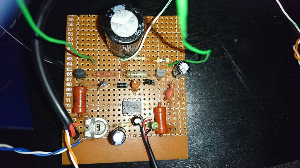
This is for you guys, who are just starting to play around with transistors and op amps. The Class B amplifier is as basic as they come, yet still has a nice and warm sound to it. It is consists of two separate stages, the first one is responsible for the voltage gain of amp and to set a correct voltage offset for output. The second part of the circuit uses power transistors to boost the current the amplifier can supply the load with. Without it, the op amp alone would start to clip the output voltage as soon as the current requirements of the load pass its current rating. As for the power supply I used an old laptop charger. Use it if you have anything lying around, It makes an appropriate power source.
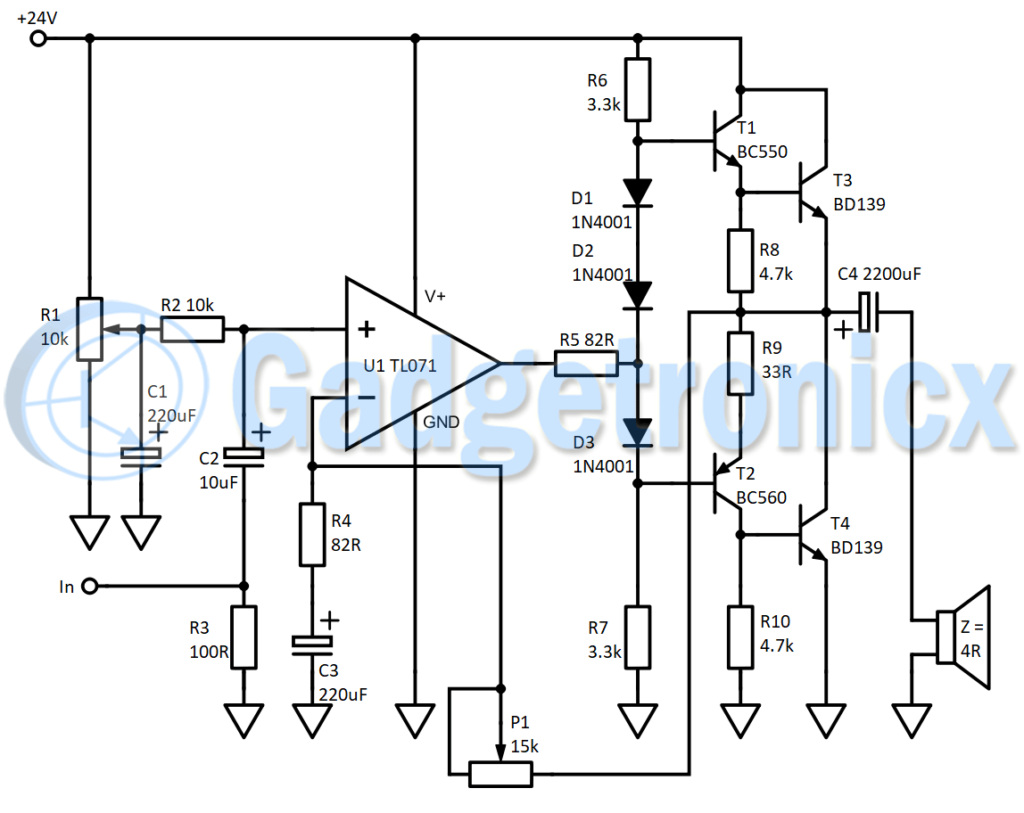
CIRCUIT DIAGRAM OF CLASS B AMPLIFIER:
VOLTAGE GAIN AND OUTPUT OFFSET REGULATION:
Op amp will handle these two parameters. I chose a very generic and common amplifier. But you can use almost any type, as long as it works with 24V supply voltage. The R1 potentiometer acts as a voltage divider, setting the output voltage of the amplifier to 1/2 the supply voltage, giving the best headroom for the amplifier to swing the output voltage. I have labeled it as a resistor for a reason, because you can actually change it to a fixed voltage divider, with 2 resistors (each 4.7k). I made it with a trimmer, because that’s what I had laying around. The voltage gain is set by the ratio between P1 and R4 plus 1. So for instance if you set P1 to 10k the gain will be (10000/82)+1=123. I strongly recommend, not setting the gain this high – keep it up to 50! .
CURRENT GAIN, POWER HANDLING AND BIAS:
The output transistors T1 and T2 form a typical darlington configuration where the current gain is set by the multiplication of the two transistors hfE. This leads to a very high current gain (typically in the range of 5000 with these transistors). Since the amplifier is a push pull Class B amp, there is a second arm of transistors which would pull at the negative portion of the input signal. I have made this pair in a somewhat unusual way (kind of old school), where the output transistor is also a NPN. This Sziklai pair, and has similar characteristics to the Darlington pair.
The reason I chose this configuration is I only had NPN power transistors, and they were paired. One might go with a PNP Darlington pair as well, with generally the same results, it comes down to what you have in your inventory. There is also one more thing to note. The 3 diodes set the bias point of the output stage at around 50mA, so that there is no crossover region between cycles, thus reducing distortion. I highly suggest keeping not skipping any of them. Even more you can add one on the lower end of the bias chain to balance out the two arms of the output stage, but this will push the bias point into the Class A region.
Hope this article would have been useful to you, do build this Class B amplifier and let me know your thoughts in the comment box below. Feel free to post your queries and comments in there as well. Happy DIY 🙂