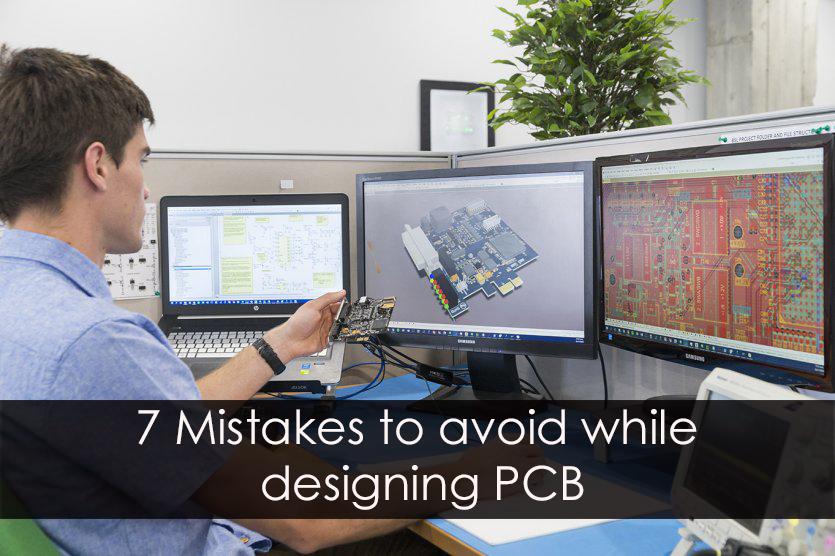
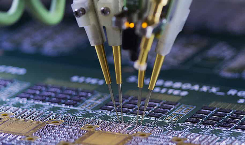
Printed circuit boards form the core of the internal of a device of electronic nature. So, designing PCB demands close attention and fool-proof approach. While trying PCB prototyping, you will find that there are a number of mistakes that we commonly encounter and even some are repetitive. These mistakes sabotage the whole purpose of circuit board design and make it look like a shabby piece of metal with components wired on it. So, it is better to know about these mistakes and carry out the PCB manufacturing process error-free so as to save time and effort in reworking.
1. Incorrect laying patterns
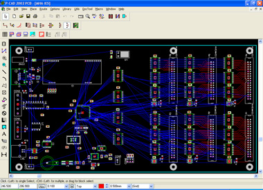
Designing PCB and prototyping has become quite an automated process with the availability of software devoted to making this task simpler. If the components are from the libraries as in the software, dealing with them becomes easier. But, if the designer chooses to go a bit experimental with the choice of components or laying patterns, then it is advisable to have a schematic diagram drawn manually first. Since, to err is a human, the manually laid landing pattern is likely to have a number of shortcomings. A simple one to mention is an error in pad to pad spacing. If this spacing goes off even by a fraction of a millimeter, the soldering process becomes difficult to carry out, thus, making PCB making more complex.
2. Very narrow designing of High current carrying traces
If the traces carrying high current are not placed wide enough, then it won’t be possible to expect it to handle the current amounting to more than a few hundred milliamps. You must know that the internal layers do not have a better capacity to handle current than the outer layers. It is because the outer ones have better heat dissipation due to enhanced air flow. Thus, proper trace width should be there so as to avoid explosion due to overheating right at the designing table.
3. Using blind or hidden vias while designing PCB
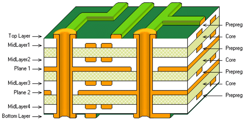
Using blind or hidden vias poses lots of difficulties while designing PCB. The hidden vias are will be within two internal layers while blind vias is to connect external layers with the internal ones. However, the way layers are stack up on the board interferes with the functionality of these vias. Therefore, many experts suggest that only through vias should be used in designing PCBs.
4. Lengthy high speed traces
If the signals need to move lightening fast, the traces must be straight and short. However, many times, the makers fail to achieve very high-speed signals due to failure to make traces short. If you plan to make products that employ PCBs run on the high-speed microprocessor, lengthy traces can come between you and your plans. So, choose correct trace length to deal with problems of poor signal transmission speed.
5. Ignoring/ wrong placement of Decoupling capacitors
Placing of the decoupling capacitor is quite crucial to the proper functioning of PCB. It is good practice to place decoupling capacitors close to the pin that requires a stable voltage supply to operate. Thus, if the decoupling capacitor is not placed on the power supply rail, the stable voltage fails to reach the pin requiring a constant power supply. Also consider using capacitors with a series inductor to create a low-pass LC filter that absorbs noise in highly sensitive devices.
6. Incorrect placement of antenna in wireless designs
The complex impedance of the antenna and transceiver must match in order to ensure maximum power transfer between them. Even the finest of electrical engineers fail to create a proper transmission line as they miss paying attention to antenna layout. A matching circuit like LC pi-network is required in between the antenna and transceiver for fine-tuning the impedance between the two. There are certain applications available to help you with antenna layout, these must be referred to so that such crucial mistakes can be avoided.
7. Improper testing and avoiding second opinions
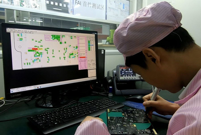
Since designing PCB is a detailed process, the designer may feel lost by the time and approaches. So, issues like hairline short-circuit etc. may lie undetected even in a PCB designed by a pro. It is, therefore, quite necessary to get the PCB tested for quality and functionality on various parameters like current flow, etc. The intricacy of design requires a look by the second eye for sure. Not discussing the design with other person leads to the prevalence of errors that ultimately may render the PCB useless. Getting the work reviewed on a regular basis can help find out shortcomings that go unnoticed on designing alone. Thus, going solo is not the correct way to design PCBs. Taking the experience of brains around help you enrich yours and takes you closer to perfection.
These are the top 7 mistakes that usually occurs with both budding or experienced professional. Learning to make good quality PCBs is possible to happen when you have some open mind and critical approach. You need to consider small factors like placement of components or width of traces while designing PCBs. These factors, no matter how menial they sound, affect the working of PCBs significantly. And eventually can lead to faulty circuit board design. Types of vias used can also contribute to list of mistakes designers usually make in creating PCB prototypes. So, learn all about these errors and try to avoid making them while designing your own PCB.

