
Illustration image
Have you ever built a super cool Hi-Fi Audio amplifier with simple components at your home? If not here is your guide to do so, am pretty sure you are gonna love this. This article narrates about making your DIY high fidelity audio amplifier with output transistor protection circuitry and 2-way speaker protection circuitry. Let’s discuss some striking features which might convince you to try making this amp.
FEATURES OF THIS Hi-Fi AUDIO AMPLIFIER:
- Input Sensitivity – 0.25mVmax – most phones output such a level.
- Input Impedance – 470ohm – solely depends on R1. You can increase R1 to whatever value you wish or exclude it altogether, but i recommend you keep it at that. Most audio cards of both laptops and phones will handle such an impedance with ease.
- Frequency Response – 1Hz – 45KHz at -3dB
- Output Power – 50Wrms or 70W musical power
- Power Consumption – 95W
- Efficiency – 53%
- Ripple Rejection – -68dB – a good value, which will attenuate power supply noise to a few hundred mV. Since the amp is in class B, there will be no substantial current draw at idle state, so the 10mF capacitors will provide exquisite filtering. When signal is applied, the hum will still be so low, that it will be inaudible.
- THD+N – 0.007@50W/1KHz – This is the value of the power amp. Due to the need of preamp, the value will be slightly higher. This value is often not topped even by the best class A amplifiers, so the amp will have virtually perfect signal recreation. This value is often indicative and may vary to some extend. Worst case scenario is 0.05%, which is still perfect for all intends of purposes. The key moment is to keep the voltage gain of the power amp low, 4 in this case.
- The output transistors of this audio amplifier are protected from excessive current draw, as one would occur if the output is shorted out while the amp is cranked up to the max. The maximum current draw is 6.3A. The protection is realized by Q13 and Q14 and all the surrounding components in their immediate vicinity.
STAGES OF Hi-Fi AUDIO AMPLIFIER:
- Power Supply Unit (PSU)
- Pre Amp Circuit
- Power amplifier and Protection circuit
POWER SUPPLY UNIT (PSU):
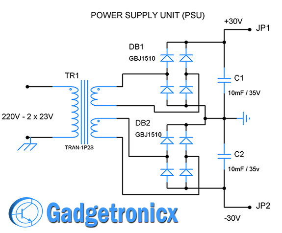
The power supply consists of normal bridge wave rectifier. A filtering capacitors C1 and C2 was used in the circuit. The values of these C1 and C2 should be no less than 10,000uF/35V. I always prefer to use 1500uF as cap value for every amp of current, this is the rule of thumb i follow. It is important to connect a heat sink to the bridges, this will keep the bridge cooler than 50 degree Celsius at 10W dissipation.
PREAMP CIRCUIT:
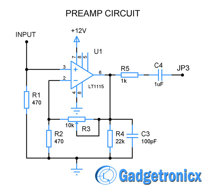
Preamp circuit was built around op-amp to boost the input signal. It is nothing but a non inverting amp with a closed loop gain of about 20. Variable resistor R3 is used adjust the gain of this preamp circuit. The boosted signal is then goes to the next stage “Power amp and Protection circuit”.
POWER AMP AND PROTECTION CIRCUIT:
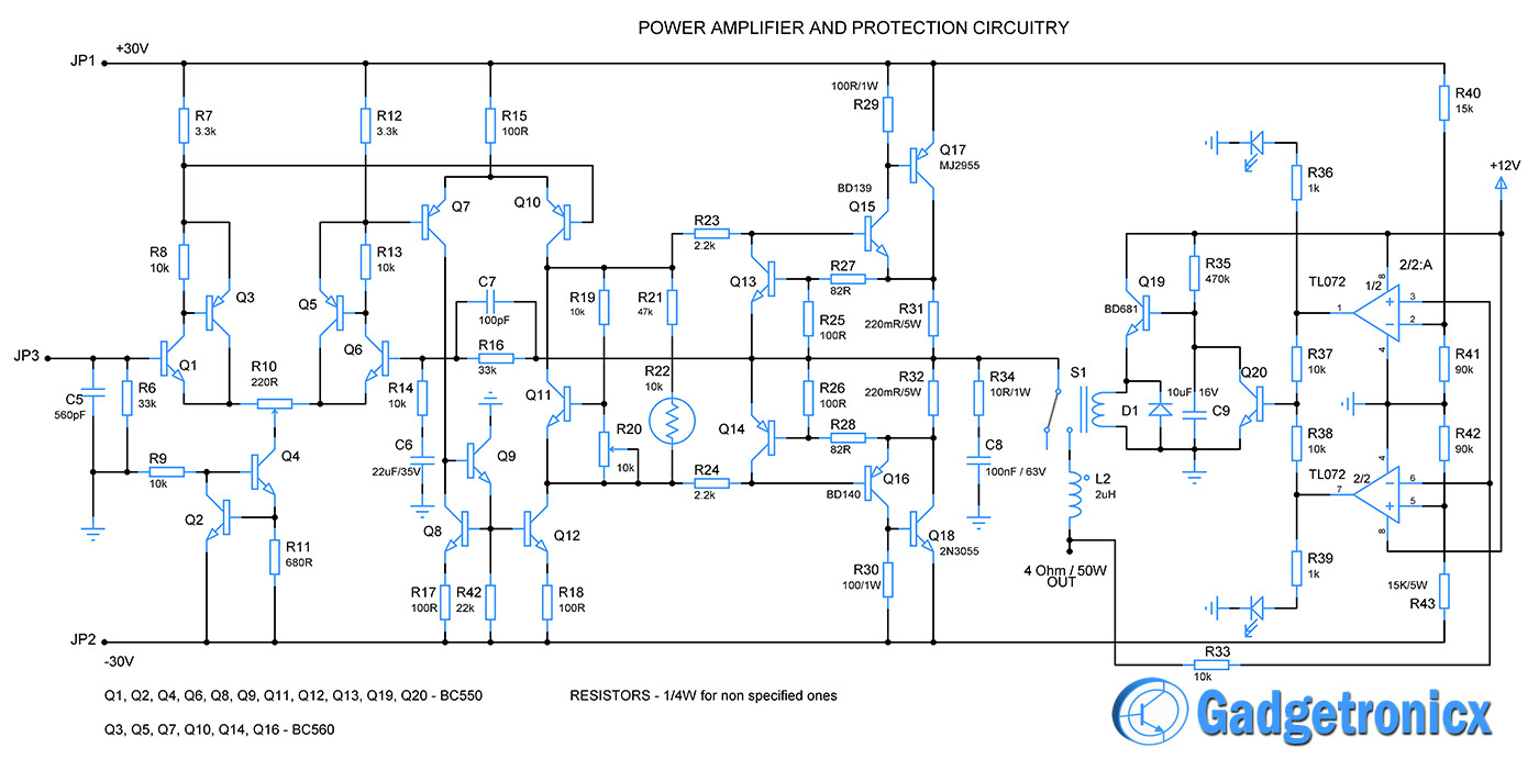
Click image to see high-resolution circuit diagram
The power amplifier takes the high impedance input signal, further amplifies it and transforms it into a low impedance signal, suitable for the speaker. The output voltage offset is set by R10 and the gain of the power amplifier is set by R14 and is currently set to 4.3. An input signal of 4.6Vmax would be enough for the full output swing.
The amplifier also incorporates two-way speaker protection. One of the protections delay the speakers from enabling for 5s after the amp has been powered up. This is to negate any peaks that may strike the speaker in the first few seconds, before all the regimes have settled down. This protects the speakers,and stops a loud popping sound, when the amp is first powered up. Another protection comprises the relay , Q19 and the delay RC chain R35,C9. I designed it for a relay that enables at 8V. Any one will do, but the turn on time will vary.
The second protection i came up with is quite interesting, and i personally haven’t seen it in any other circuits. This circuit comprises the two most right op amps (they come in one package) and Q20 and protects the speakers if any of the power transistors fail. Usually this will expose the speakers to the full voltage of one of the rails (30V) , which may be catastrophic for speakers and diode bridges. So the bottom line is that it should absolutely be avoided.
How it works, you may ask. The two op-amps work as comparators. One end is set at a voltage close to the rail voltage. You can choose any voltage between 22V and 28V set by R38/R39 and R40/R41. I`ve chosen a voltage of around 26V. So, since the output in a normal operation will never exceed 0.707 of the max rail voltage (21Vmax) it is safe to assume, that during a normal operation, no false triggering will occur.
Just in case if one of the power transistors fail, it most often becomes a short-circuit. That exposes the speaker and the other input of the respectful comparator to a voltage higher than the reference voltage (26V). This causes the op amp to trigger the Q20 transistor, which then fully discharges C9, the capacitor that keeps the relay driving transistor on, thus cutting the connection to the speaker. This protection is very fast (50-60ms) and is superior than a simple fuse protection, which may keep the short for up to 1s.
Temperature drift compensation by Q11 and R22 thermistor. Both should be mounted close to the heat sink or somehow glued to it. The increasing temperature will cause the output voltage to drift around the 0V offset, so the temperature dependence of the thermistor and the Q11 transistor, will keep the voltage centered around 0V, or will partially null this effect. Usually a little more complex system is used, but this amp is only rated 50W, so even this will do the trick.
TIPS AND RECOMMENDATIONS:
- The most important tip i have to give you is to never exclude C6. It ( with conjunction with C4) are the two components that ensure the amplifier stability and keep its tendency to oscillations at bay.
- Use the closest matched transistors from the BCxxx in the circuit, that you can get. Just buy 40-50 of the BC550 ( they are extremely cheap) and like 10-20 of the BC560 and test them all, and choose only ones with the closest hFe you can get.
- Also use very low tolerance resistors, the 3.3k resistors should have a 1% tolerance.
- Since it’s virtually impossible to match all components i have added R10, which is used to fine tune the output voltage offset. Using it, set the offset closest to 0V as possible. To do so, don’t use a voltmeter at the output. they tend to be somewhat inaccurate, instead use a mA meter in series with the load. Once you’ve hit the closest you can get to 0mA, that’s your center point.
- The circuit is designed to only be able to handle 50W of power. If you want to get more out of it, you will need to put another pair of the output transistors in parallel, increase the power supply rails and increase the gain of the power amp by lowering the value of R14. Keep in mind that the transistors chosen are for this voltage levels and they will not work at a differential voltage more than 80V. The maximum voltage you can obtain is 0,7 of the Vcc, therefore the maximum power is (0,707.Vcc)^2/Rl.
- You must provide a sufficient heat sink to keep the power transistors cool. Keep the thermistor and Q11 close or even glued onto the heat sink, They are the temperature drift compensation components.
- Set the current through the power transistors to 20mA by R20
- Set the output voltage offset to closest to 0V you can, by R10, keep the amp running at max output for 20min or so and readjust if necessary.
- The diode bridges must also be mounted on sufficient heatsink to handle roughly 10W-15W of power dissipation
- Use a star-shaped ground layout topology for lowest hum
FIRST POWER-UP INSTRUCTIONS:
- After assembling the circuit, make sure everything is soldered correctly and add all the heat sinks.
- Set R20 somewhere in the middle position.
- Add a dummy load. Just use a 1W/4ohm resistor submerged in pure water.
- Power it up. Set your voltmeter to the 20mV scale, and measure the voltage drop from one of the 220mOhm resistors. Adjust R20 until you see a reading of around 5mV. This means that the idle current of the power transistors is set at around 25mA. This sets the amp in the class B region. If you want to push it further in the class AB region (which I do recommend) just adjust R20 until you get a reading of 25mV. This means that the idle current is set around 100mA.
- Measure the output voltage. Use R10 to adjust the offset until you get it as close to 0V as you can.
- Inject an input signal (preferably sine wave) or something from the source you’re gonna use the most, keeping the water cooled load, and use an oscilloscope on the output. Adjust the preamp gain until you get a non clipped sine wave on the output, and keep the amp running at maximum power for a while (15-20min) and then remove the input signal. Measure the output voltage offset again, and readjust by R10 again.
- Restart the amp again and see if everything is working as it should, if not retrace your steps and readjust again.
Hope you all like this project, please feel free to post your queries in the comment section below.


this protection power supply and preamp circuits have nothing to do with original gainclone PA100 amplifier that has regulated psu, no preamp and protection circuit built in output chipamps.
Regarding your protection circuit, you reference R38/39 but should say R42/43. By the way, you are setting these ref voltages well above the opamp rails and not only will the comparator function not work, but this will overstress the inputs. Additionally you have the opamp powered from only +12V instead of +/-12V but even then you will likely blow up the inputs by biasing them at +/-26V. It also seems a bit excessive to require the input signal (amplifier output) to go to 26V before you trip the relay. Most woofers have a DCR of 5 to 6 ohms, which is 5 amps! Have you actually built the circuit? Tested it?
Parts list with sources ? Where did you get the torroid?
Pcb please
A few remarks:
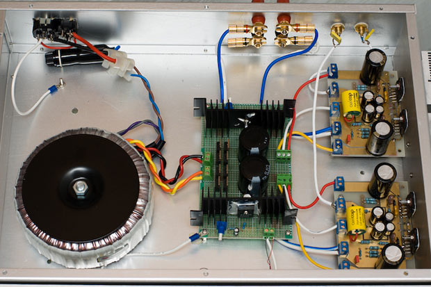
1. MJ2955 and 2N3055 (it’s been around since 1960s) have large metal TO3 packages which need a heatsink with a special layout of holes. There’s a more modern equivalent named TIP2955/TIP3055 in TO-247 package, meaning that it can be soldered directly into the PCB and attached to the heatsink, like the amp in the picture has.
2. +12V can be taken from the +30V rail through a 7812 voltage regulator.
3. Use a +/-12V or +/-15V (again, via 78xx and 79xx regulators) symmetrical supply for the LT1112 opamp. This way it’ll stay at 0V DC instead of +6V DC, and you no longer have to use the coupling capacitor (C4). R1 has a very low value (470 ohms) which makes it unsuitable for anything other than a low-impedance dynamic microphones (typically 200 ohms); it can be safely replaced with 47k.
4. Instead of using two rectifier bridges, you can connect the beginning of one winding and the end of the other one directly to the ground. The other ends will then go to a single bridge (with + connected with the positive rail, and – connected with the negative rail). This will raise the rail voltage by 0.7V (e.g. +/-30.7V) which allows a little bit more output power.
5. When powering up an amplifier for the first time, connect a reasonably large light bulb (100W or even more) in series with the mains supply. When anything bad happens (e.g. the amp goes into oscillation, a short circuit on a rail supply, or a damaged output transistor, etc.), the bulb will limit the power going into the amp, possibly saving some components from damage. If it doesn’t light up, the amplifier might work OK; it’s time to set the quiescent current and test the thing.